
A large number of op amp parameters are listed in the datasheet of the general op amp. Some are easy to understand, we are always concerned, and some may be ignored. In the next few topics, each parameter will be described and analyzed in detail. Try to clarify the parameters of the op amp on the principle and the impact on the application. Due to my limited level, it is inevitable that there will be some omissions in the written blog post. I hope everyone will criticize and correct.
The first section describes the op amp's input bias current Ib and the input offset current Ios. It is well known that the ideal op amp has no input bias current Ib and input offset current Ios. But each actual op amp will have an input bias current Ib and an input offset current Ios. We can use the model in the figure below to illustrate their definition.
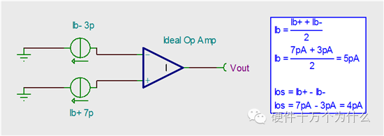
The input bias current Ib is due to the presence of leakage current (which we will call leakage current) at both input poles of the op amp. We can understand that the input terminals of the ideal op amp are connected in series with a current source, and the current values ​​of the two current sources are generally different. That is to say, in actual operation, there will be current flowing into or out of the input of the op amp (not the same as the virtual amp of the ideal op amp). Then the input bias current defines the average of these two currents, which is well understood. The input offset current is defined as the difference between the two currents.
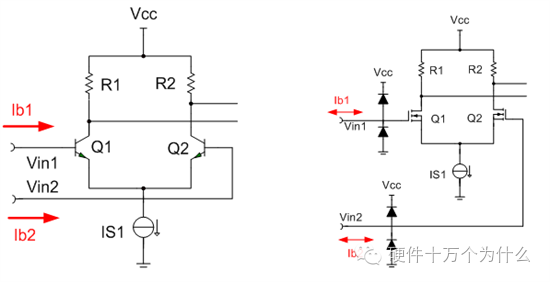
After the definition, let's take a look at the source of this current. Then we have to look at the input stage that is shipped in. The input stage of the op amp typically uses a differential input (voltage feedback op amp). The tube used is either a bipolar bipolar or a FET FET. As shown in the figure below, for bipolar, to make it work in the linear region, it is necessary to provide a bias voltage to the base, or to have a relatively large base current. It is also said that the triode is a current control device. Then the bias current is derived from the base current of the triode in the input stage. Since it is difficult to completely match the two tubes in the process, the base currents of the two tubes Q1 and Q2 always have such a difference. That is the input offset current. The two values ​​of the oppolar input op amp are still considerable, that is to say, they are relatively large, and have to be considered when designing the circuit. For the FET input op amp, because it is a voltage-controlled current device, it can be said that its gate current is very small, usually in the fA level, but unfortunately, each of its input pins has a Protection diode for ESD. Both of these diodes have leakage currents. This leakage current is generally much larger than the gate current of the FET, which is also the source of the bias current for the FET input op amp. Of course, the two pairs of ESD protection diodes are not completely identical, so there are different leakage currents, and the difference between the leakage currents constitutes the main component of the input offset current.
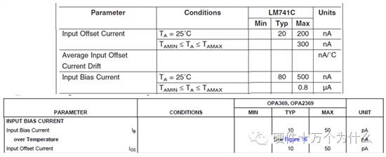
The table above is the input bias current and input offset current of the bipolar LM741. This current flows to the external resistor. Even if it is K-class, it will generate an offset voltage of several tens of uV. After amplification, it is easy to Will cause the output voltage error to mV level. The following table shows the input bias current and input offset current of the CMOSFET's OPA369. These two values ​​are much smaller. The better value of the better COMS op amp input bias current and input offset current can be less than 1pA. aims.
It is also emphasized here that the reverse leakage current of the ESD is related to its reverse voltage. Therefore, when Vin=(Vcc-Vss)/2, the voltage applied to the two ESD protection diodes is equivalent, and their reverse currents can be considered to be approximately equal. Ideally, no current flows in or out. Is the current reaches a minimum. Therefore, there is a minimum bias current. When the voltage at the input of the op amp is not equal to (Vcc-Vss)/2, it will inevitably cause the reverse voltage of one diode to be high and the other to be low. The current is not equal, and this difference current constitutes the main component of the input bias current. This scene is called the collar effect. Therefore, to minimize the FET input bias current, set the common-mode voltage to (Vcc-Vss)/2.
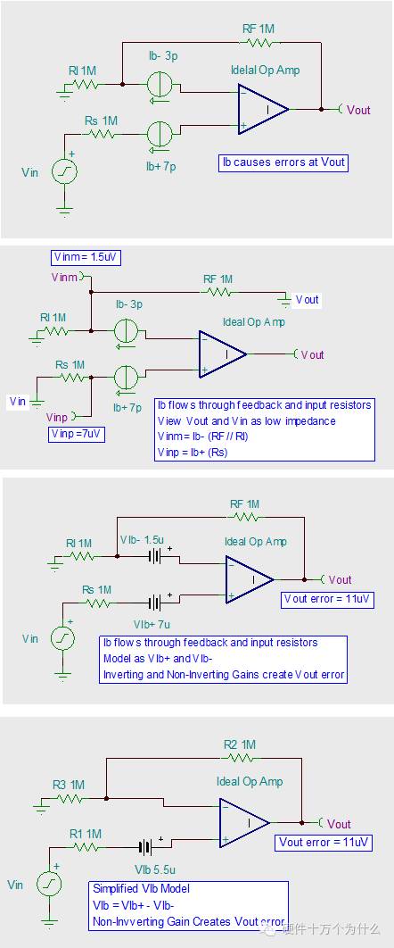
The definitions and sources are analyzed above. Let's talk about the influence of these two parameters on the circuit. The input bias current will flow through the external resistor network, which will be converted into the offset voltage of the op amp. After the operation, it will reach the output of the operation. The input error of the op amp is caused. This also explains why, in the reverse amplifier circuit, why a resistor is connected to the non-inverting input of the op amp. And this resistance should be equal to the value of the reverse input and the feedback resistor in parallel. This is to make the two input terminals bias current flow through the resistor, the voltage values ​​are equal, so that they introduce an offset voltage of zero. To put it this way, it is too abstract, but it is easy to understand some of the following diagrams.
Another point is that for the circuit of small current detection, it is generally a transimpedance amplifying circuit, such as a photodiode detecting circuit. Generally, the optical power signal which is relatively weakly converted by the optical signal is weaker, and is often nA level rather than pA level. The intention of this circuit is to let the photocurrent flow to the feedback resistor to generate a voltage at the output of the amplifier circuit. If the op amp's input bias current is too large, just a portion of this faint photo current will flow into the op amp's input without a preset I/V linear conversion.
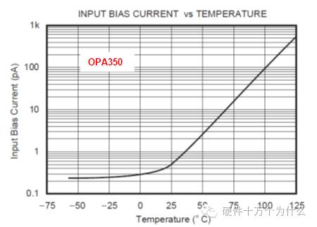
Also note that many of the op amp's input offset currents vary with temperature. As shown in the figure below, the OPAl350's input offset current rises rapidly above 25 degrees. The input bias current at 100 degrees is several hundred times that of 25 degrees. If the system is designed to operate over a wide temperature range, this factor has to be considered.
The above mentioned the input bias current and offset current of the op amp, I hope to be useful to everyone.
Toggle Switches,Waterproof Toggle Switch,Waterproof Rocker Switch,Mini Toggle Switch
Lishui Trimone Electrical Technology Co., Ltd , https://www.3gracegfci.com