
Audio Amplifier The purpose of the background audio amplifier is to reproduce true, efficient, and low distortion input audio signals on the vocal output components at the required volume and power levels. The audio frequency range is approximately 20 Hz to 20 kHz, so the amplifier must have a good frequency response over this frequency range (the frequency range is reduced when driving a speaker with a limited band, for example, a woofer or tweeter). Output power capability varies widely depending on the application, from milliwatts (mW) of headphones, several watts (W) of TV (TV) or personal computer (PC) audio, tens of watts of "mini" home audio and cars Audio, home and commercial audio systems with high powers of hundreds of watts and hundreds of watts, and theater or concert hall sound systems.
A direct analog implementation of an audio amplifier uses a transistor to produce an output voltage proportional to the input voltage in a linear mode of operation. The forward voltage gain is typically very high (at least 40 dB). If the forward gain is part of the feedback loop, then the total loop gain will also be high. Feedback loops are often used because high loop gain improves performance, rejects distortion due to linearity errors in the forward path, and reduces power supply noise by increasing power supply rejection (PSR).
Advantages of Class D Amplifiers In conventional transistor amplifiers, the output stage contains transistors that provide instantaneous continuous output current. Many possible types of audio system amplifiers are available, including Class A amplifiers, Class AB amplifiers, and Class B amplifiers. Compared to Class D amplifier designs, even the most efficient linear output stage, their output stage consumes a lot of power. This difference makes Class D amplifiers a significant advantage in many applications because low power generates less heat, saves printed circuit board (PCB) area and cost, and extends battery life in portable systems.
The linear amplifier, class D amplifier, and power linear amplifier output stage are directly connected to the speaker (in some cases connected by a capacitor). If the output stage uses bipolar junction transistors (BJTs), they typically operate in a linear fashion with large collector voltages. The output stage can also be implemented with a complementary metal oxide semiconductor (CMOS) transistor, as shown in Figure 1.
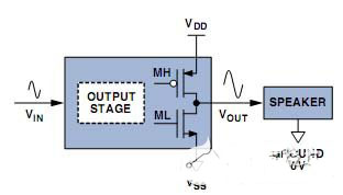
Figure 1. CMOS linear output stage
Power consumption is at all linear output stages because the process of generating the output voltage VOUT inevitably results in non-zero IDS and VDS in at least one of the output transistors. The amount of power consumed depends primarily on the biasing method on the output transistors.
Class A amplifier topologies use a single transistor as a direct current (DC) current source that provides the maximum audio current required by the speaker. Class A amplifier output stage can provide excellent sound quality, but the power consumption is very large, because usually there is a large DC bias current flowing through the output stage transistor (which we do not expect), but not provided to the speaker (this is us Expected).
Class B amplifier topologies have no DC bias current, so power consumption is greatly reduced. Its output transistors are independently controlled by push-pull, allowing the high-side transistors to supply positive current to the speaker and the low-side transistors to sink negative current. Since only the signal current flows through the transistor, the output stage power consumption is reduced. However, the quality of the Class B amplifier circuit is poor because it causes a linearity error (crossover distortion) when the output current crosses zero and the transistor switches between on and off states.
Class AB amplifiers are a combination of Class A and Class B amplifiers. They also use DC bias current, but they are much smaller than pure Class A amplifiers. The small DC bias current is sufficient to prevent crossover distortion and thus provide good sound quality. Its power consumption is between Class A and Class B amplifiers, but is usually closer to Class B amplifiers. Similar to Class B amplifier circuits, Class AB amplifiers also require some control circuitry to provide or sink large output currents.
Unfortunately, even a well-designed Class AB amplifier consumes a lot of power because the output voltage in the range is usually far from the positive or negative supply. Since the voltage drop between the drain and the source is large, a large instantaneous power consumption IDS × VDS is generated.
Class D amplifiers have much lower power consumption than any of the above types of amplifiers due to their different topologies (see Figure 2). The output stage of the Class D amplifier switches between a positive supply and a negative supply to generate a series of voltage pulses. This waveform is advantageous for reducing power consumption because the output transistor has zero current when it is not conducting, and has a very low VDS when turned on, thus generating a small power consumption IDS × VDS.
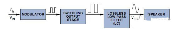
Figure 2. Block Diagram of a Class D Open Loop Amplifier
Since most audio signals are not bursts, a modulator must be included to convert the audio input into a pulsed signal. The frequency components of the pulse include the desired audio signal and the important high frequency energy associated with the modulation process. A low pass filter is often inserted between the output stage and the speaker to minimize electromagnetic interference (EMI) and to avoid driving the speaker with too much high frequency energy. In order to maintain the power consumption advantages of the switching output stage, the filter (see Figure 3) is required to be lossless (or nearly lossless). Low-pass filters typically use capacitors and inductors, and only the speaker is an energy-consuming component.

Figure 3. Differential Switch Output Stage and LC Low Pass Filter
Figure 4 compares the ideal value of the Class A and Class B amplifier output stage power dissipation (PDISS) with the measured value of the AD1994 Class D amplifier output stage power dissipation. The curve in the figure refers to the relationship between the output stage power of a given audio sine wave signal and the load power (PLOAD) provided by the speaker. The load power is normalized to the maximum load (PLOAD max) power level, and the clamped sine wave signal guarantees 10% total harmonic distortion (THD). The vertical line in the figure indicates where PLOAD begins to clamp.
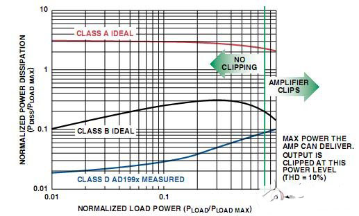
Figure 4. Power Comparison of the Output Stages of Class A, Class B, and Class D Amplifiers
It can be seen that the power consumption is significantly different for a variety of loads, especially at high end and mid-range load conditions. At the beginning of the clamp, the Class D amplifier output stage consumes approximately 1/2.5 of the Class B amplifier and is 1/27 of the Class A amplifier. It should be noted that the power consumed in the output stage of the Class A amplifier is greater than the power delivered to the speaker, which is the result of using a large DC bias current.
The output stage power efficiency Eff is defined as follows:
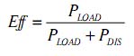
At the beginning of the clamp, the Eff of the Class A amplifier is 25%, the Eff of the Class B amplifier is 78.5%, and the Eff of the Class D amplifier is 90% (see Figure 5). These best examples are often cited in textbooks for Class A and Class B amplifiers.
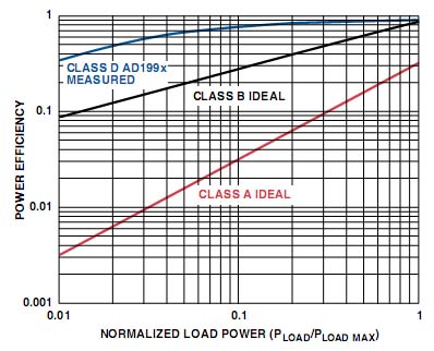
Figure 5. Power efficiency comparison of Class A, Class B, and Class D amplifier output stages
The difference in power consumption and power efficiency is large at medium power levels. This is important for audio because the long-term average power level of loud music is much lower than the instantaneous peak level of PLOAD max (1/5 to 1/20, depending on the type of music). Thus, for an audio amplifier, [PLOAD = 0.1 × PLOAD max] is a reasonable average power level at which PDISS is evaluated. At this power level, the power dissipation of the Class D amplifier output stage is 1/9 of that of a Class B amplifier and 1/107 of a Class A amplifier.
For a 10 W PLOAD max audio amplifier, an average PLOAD of 1 W is considered a fidelity audio power level. Under these conditions, the Class D amplifier output stage consumes 282 mW internally, which is 2.53 W for Class B amplifiers and 30.2 W for Class A amplifiers. In this case, the efficiency of the Class D amplifier is reduced from 90% to 78% under high power conditions. But even 78% is far superior to Class B and Class A amplifiers, with efficiencies of 28% and 3%, respectively.
These differences have an important impact on system design. For power levels above 1 W, excessive power dissipation in the linear output stage requires an effective heat dissipation method to avoid unacceptable heat generation, typically using a large metal plate as a heat sink or a fan to facilitate amplifier air dissipation. If the amplifier is an integrated circuit (IC), a large, costly, thermally enhanced package may be required to facilitate heat transfer. These considerations are cumbersome in consumer products, such as flat-panel TVs, where printed circuit board area (PCB) area is valuable, or car audio, and the trend is to increase the number of channels in a fixed space.
For power levels below 1 W, dealing with wasted power may be more difficult than handling heat. If battery powered, the linear amplifier output stage consumes more battery charge than a Class D amplifier. In the above example, the power supply current of the Class D amplifier output stage is 1/2.8 of the Class B amplifier, which is 1/23.6 of the Class A amplifier, so they are used in batteries such as cellular phones, PDAs and MP3 players. There is a big difference in life.
So far, for the sake of simplicity, we have only focused on the analysis of the amplifier output stage. But when considering all the power consumption in an amplifier system, a linear amplifier is more advantageous than a low output power class D amplifier. The reason is that at low power levels, the power required to generate and modulate the switching waveform can be large. Thus, the wide system static power advantages of well-designed low- and medium-power Class AB amplifiers make them competing with Class D amplifiers. Although for a wide output power range, there is no doubt that Class D amplifiers have a low power consumption advantage.
Class D Amplifier Terminology and Comparison of Differential and Single-Ended Modes Figure 3 shows the differential implementation of the output transistors and LC filters in a Class D amplifier. This H-bridge has two half-bridge switching circuits that provide pulses of opposite polarity to the filter, where the filter contains two inductors, two capacitors, and a speaker. Each half bridge contains two output transistors, one connected to the high side transistor MH of the positive supply and the other connected to the low side transistor ML of the negative supply. Shown in Figure 3 is a high side pMOS transistor. High-end nMOS transistors are often used to reduce size and capacitance, but special gate drive methods are required to control them (see in-depth reading 1).
The full H-bridge circuit is typically powered by a single supply (VDD) and the ground is used to connect to the negative supply (VSS). For a given VDD and VSS, the differential mode of the H-bridge circuit provides twice the output signal in a single-ended manner and four times the output power. The half-bridge circuit can be powered by a bipolar supply or a unipolar supply, but a single supply can potentially harm the DC bias voltage because only the VDD/2 voltage is applied to the overdrive unless a DC blocking capacitor is added.
The "excited" half-bridge circuit supply voltage bus can exceed the nominal value produced by the LC inductor's large inductor current. An increased decoupling capacitor between VDD and VSS can limit the transient variation of the excitation dV/dt. The full-bridge circuit is unaffected by bus excitation because the inductor current flows in from one half-bridge and out of the other, causing the local current loop to have minimal interference to the power supply.
Audio Class D Amplifier Design Factors While leveraging the low power consumption of Class D amplifiers to power its audio applications, there are some important issues that design engineers need to consider, including:
â— Output transistor size selection â— Output stage protection â— Sound quality â— Modulation method â— Anti-electromagnetic interference (EMI)
◠LC Filter Design ◠System Cost Output Transistor Size Selection The output transistor size is chosen to reduce power consumption over a wide range of signal conditioning. When conducting a large IDS, the VDS is guaranteed to be small, and the on-resistance (RON) of the output transistor is required to be small (typically 0.1 Ω to 0.2 Ω). But this requires a large transistor with a large gate capacitance (CG). The power consumption of the switched capacitor gate drive circuit is CV2f, where C is the capacitor, V is the voltage change during charging, and f is the switching frequency. If the capacitance or frequency is too high, this "switching loss" will be too large, so there is a practical upper limit. Therefore, the choice of transistor size is a compromise between minimizing IDS x VDS losses during conduction and minimizing switching losses. At high output power, power consumption and efficiency are primarily determined by conduction losses, while at low output power, power consumption is primarily determined by switching losses. Power transistor manufacturers attempt to minimize the RON x CG of their devices to reduce the total power consumption in switching applications, providing flexibility in switching frequency selection.
The output stage protection output stage must be protected from many potentially hazardous conditions:
Overheating: Although the output power of a Class D amplifier is lower than that of a linear amplifier, if the amplifier provides very high power for a long time, it will still reach the level of the output transistor. In order to prevent the risk of overheating, a temperature monitoring control circuit is required. In a simple protection scheme, when the temperature measured by an on-chip sensor exceeds the thermal shutdown safety threshold, the output stage is turned off and remains cool until it is cooled. In addition to a simple binary indication that the temperature has exceeded the shutdown threshold, the sensor can provide additional temperature information. By measuring the temperature, the control circuit can gradually reduce the volume level, reduce power consumption and maintain the temperature well within a defined range, rather than forcing no sound during thermal shutdown.
Output transistor overcurrent: If the output stage and the speaker terminal are properly connected, the output transistor has a low on-resistance state without problems, but if these nodes are not careful to short-circuit with another node or positive and negative power supplies, it will generate a huge Current. If not verified, this current will destroy the transistor or peripheral circuitry. Therefore, a current detection output transistor protection circuit is required. In a simple protection scheme, if the output current exceeds the safety threshold, the output stage is turned off. In more complicated scenarios.
The current sensor output is fed back into the amplifier in an attempt to limit the output current to a maximum safe level while allowing the amplifier to operate continuously without shutting down. In this scenario, if the current limit protection is invalid, the last resort is to force a shutdown. An effective current limiter also keeps the amplifier safe when a temporary large transient current occurs due to speaker resonance.
Undervoltage: Most switching output stage circuits only work when the positive supply voltage is high enough. If the power supply voltage is too low, an undervoltage condition will occur and problems will occur. This problem is usually handled by an undervoltage lockout circuit that allows the output stage to operate only when the supply voltage is greater than the undervoltage lockout threshold.
Output transistor turn-on timing: The MH and ML output stage transistors (see Figure 6) have very low on-resistance. Therefore, it is important to avoid simultaneous conduction of MH and ML because it generates a low-resistance path from VDD to VSS through the transistor, which produces a large inrush current. The best case is when the transistor is hot and consumes power; in the worst case, the transistor can be destroyed. The first turn-on and turn-off control of the transistor prevents the inrush current condition from occurring by forcing both transistors to turn off before one transistor turns on. The time interval in which both transistors are turned off is called non-overlap time or dead time.
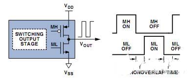
Figure 6. The first step and the back switch of the output stage transistor
Sound quality In class D amplifiers, several problems must be solved in order to achieve good overall sound quality.
“咔嗒â€: The hum that is emitted when the amplifier is turned on or off is very annoying. Unfortunately, they are easy to introduce into Class D amplifiers unless special attention is paid to modulator state, output stage timing, and LC filter state when the amplifier is muted or not muted.
Signal-to-Noise Ratio (SNR): To avoid clicks from the noise floor of the amplifier, the SNR should typically exceed 90 dB for low power amplifiers in portable applications and 100 dB for medium power designs, which should exceed for high power designs. 110 dB. This is achievable for a variety of amplifiers, but specific noise sources must be tracked during amplifier design to ensure a satisfactory overall SNR.
Distortion Mechanism: The distortion mechanism includes the nonlinearity in the modulation technique or modulator implementation, and the dead time used by the output stage to solve the inrush current problem.
Information containing the amplitude of the audio signal is typically encoded in the output pulse width of the class D modulator. The dead time used to prevent the output stage inrush current is added introduces a nonlinear timing error that is proportional to the timing error produced by the speaker relative to the ideal pulse width. The shortest dead time to avoid impact is often the most beneficial for minimizing distortion; for a detailed design methodology to optimize the distortion performance of the switching output stage, see in-depth reading 2.
Other sources of distortion include: mismatch in rise and fall times of the output pulse, mismatch in timing characteristics of the output transistor gate drive circuit, and nonlinearity of the LC low-pass filter components.
Power Supply Rejection (PSR): In the circuit shown in Figure 2, the power supply noise is almost directly coupled to the output speaker with minimal suppression. This happens because the output stage transistor connects the power supply to the low pass filter through a very low resistance. The filter rejects high frequency noise, but all audio frequencies pass, including audible noise. See Section 3 for a detailed description of the effects of power supply noise on single-ended and differential-switched output stage circuits.
If the distortion problem and the power supply problem are not solved, it is difficult to achieve a PSR better than 10 dB, or a total harmonic distortion (THD) better than 0.1%. Even worse, THD tends to be high-order distortion of harmful sound quality.
Fortunately, there are some good solutions to solve these problems. Using feedback with high loop gain (as used in many linear amplifier designs) is very helpful. Feedback from the LC filter input greatly increases the PSR and attenuates all non-LC filter distortion sources. The LC filter nonlinearity can be attenuated by the speakers included in the feedback loop. High-fidelity sound quality of PSR "60 dB and THD <0.01% can be achieved in a well-designed closed-loop Class D amplifier.
However, the feedback complicates the design of the amplifier because the stability of the loop must be met (a very complex consideration for high-order designs). Continuous time analog feedback is also necessary to capture important information about pulse timing errors, so the control loop must include analog circuitry to process the feedback signal. This can increase die cost in integrated circuit amplifier implementations.
To minimize IC cost, some manufacturers prefer not to use or use the least amount of analog circuitry. Some products use a digital open-loop modulator and an analog-to-digital converter to detect power supply variations and adjust the modulator behavior to compensate, as described in In-Depth 3. This will improve the PSR, but will not solve any distortion problems. Other digital modulators attempt to pre-compensate for expected output stage timing errors or to correct non-ideal modulators. This will handle at least some of the distortion sources, but not all. Applications with loose sound quality can be processed with these open-loop Class D amplifiers, but for the best sound quality, some form of feedback seems to be required.
Modulation Technology Class D Amplifier Modulators can be implemented in a variety of ways, with extensive research and intellectual property support. This article only covers the basic concepts.
All Class D amplifier modulation techniques encode information about the audio signal into a series of pulses. Typically, the pulse width is related to the amplitude of the audio signal, which includes useful audio signal pulses and unwanted (but unavoidable) high frequency components. In all scenarios, the total integrated high frequency power is approximately the same because the total power of the waveform in the time domain is the same, and according to the Parseval theorem, the time domain power must be equal to the frequency domain power. However, the energy distribution varies greatly: in some scenarios, there is a high energy tone above the low noise floor, while in other schemes, the energy is shaped to eliminate high energy tones, but the noise floor is higher.
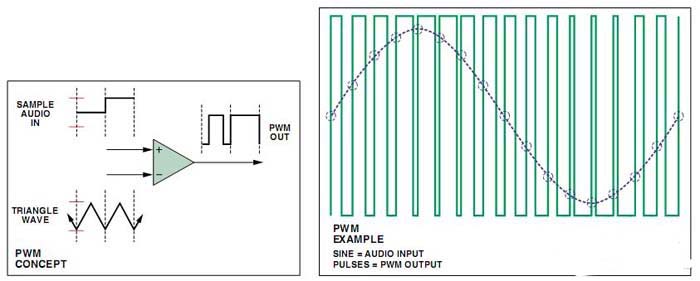
The most common modulation technique is Pulse Width Modulation (PWM). In principle, PWM compares an input audio signal with a triangular or ramp wave operating at a fixed carrier frequency. This produces a series of pulses at carrier frequency conditions. The duty cycle of the PWM pulse is proportional to the amplitude of the audio signal during each carrier cycle. In the example of Figure 7, both the audio input and the triangular wave are centered at 0 V, so for zero input, the duty cycle of the output pulse is 50%. For large positive inputs, the duty cycle is close to 100%, and for large negative inputs, the duty cycle is close to 0%. If the amplitude of the audio exceeds the amplitude of the triangular wave, full modulation occurs, at which point the pulse train stops switching and the duty cycle is 0% or 100% over a specific period.
PWM is attractive because it allows 100 dB or better audio band SNR at a few hundred kilohertz PWM carrier frequency (sufficiently low to limit output stage switching losses). Many PWM modulators are also stable with almost 100% modulation, which in principle allows high output power to reach the point of overload. However, there are several problems with PWM: First, the PWM process adds inherent distortion in many implementations (see in-depth reading 4). Second, the resonance of the PWM carrier frequency produces EMI in the amplitude-modulated (AM) radio band. Finally, The PWM pulse width is very small near the full modulation. This causes problems in most switching output stage gate drive circuits because their drive capability is limited and cannot be properly switched with the extreme speed required to regenerate a few nanoseconds (ns) of short pulse width. Therefore, in PWM-based amplifiers, full modulation is often not achieved, and the maximum achievable output power is less than the theoretical maximum, that is, only the supply voltage, transistor on-resistance, and speaker impedance are considered.
An alternative to PWM is Pulse Density Modulation (PDM), where the number of pulses in a given time window (pulse width) is proportional to the average of the input audio signal. Its individual pulse width is not as arbitrary as PWM, but rather a "quantization" multiple of the modulator clock period. 1 bit Σ-Δ modulation is a form of PDM.
A large amount of high-frequency energy in sigma-delta modulation is distributed over a wide frequency range, rather than being concentrated at the frequency multiplier of the carrier frequency like PWM, so the potential EMI advantage of sigma-delta modulation is better than PWM. At the image frequency of the PDM sampling clock frequency, energy still exists; but in the typical clock frequency range of 3 MHz to 6 MHz, the image frequency falls outside the audio band and is strongly attenuated by the LC low-pass filter.
Another advantage of sigma-delta modulation is that the minimum pulse width is one sample clock period, even for signal conditions that are close to full modulation. This simplifies the gate driver design and allows safe operation at full power in theory. Nonetheless, 1-bit sigma-delta modulation is not commonly used in Class D amplifiers (see in-depth data 4) because traditional 1-bit modulators can only be stabilized to 50% modulation. At least 64 times oversampling is also required to achieve sufficient audio band SNR, so a typical output data rate is at least 1 MHz and power efficiency is limited.
Self-oscillating amplifiers have recently been developed, such as one described in In-Depth 5. This type of amplifier always includes a feedback loop that determines the switching frequency of the modulator based on the loop characteristics, replacing the externally supplied clock. High frequency energy is often flatter than the PWM distribution. Since the effect of feedback can achieve excellent sound quality, the loop is self-oscillating, so it is difficult to synchronize with any other switching circuit, and it is difficult to connect to a digital audio source without first converting a digital signal into an analog signal.
Full-bridge circuits (see Figure 3) can use "three-state" modulation to reduce differential EMI. In the traditional differential mode of operation, the output polarity of half-bridge A must be opposite to the output polarity of half-bridge B. There are only two differential operating states: output A high, output B low; output A low, output B high. However, there are two other common mode states, that is, the two half bridge outputs have the same polarity (both high or low). One of the two common mode states can be combined with the differential state to produce a three-state modulation, and the differential input of the LC filter can be positive, zero or negative. The zero state can be used to represent a low power level, replacing the switch between the positive and negative states in a two-state scheme. During the zero state, the LC filter's differential action is very small, while actually increasing common mode EMI, but reducing differential EMI. The differential advantage applies only to low power levels because the positive and negative states must still be used to provide high power to the speaker. The varying common mode voltage levels in a three-state modulation scheme is a design challenge for closed-loop amplifiers.
Dry goods sharing: engineers teach you how to design class D amplifiers
The high frequency component of the EMI processing class D amplifier output deserves serious consideration. If not properly understood and processed, these components can generate a lot of EMI and interfere with the work of other devices.
Two types of EMI need to be considered: signals that radiate into space and signals that are conducted through the speaker and power lines. The Class D amplifier modulation scheme determines the baseline spectrum of the conducted EMI and radiated EMI components. However, some board-level design methods can be used to reduce the EMI emitted by a Class D amplifier, regardless of its baseline spectrum.
A useful principle is to minimize the area of ​​the loop carrying the high frequency current because the strength associated with EMI is related to the loop area and the proximity of the loop to other circuits. For example, the layout of the entire LC filter (including speaker wiring) should be as tight as possible and kept close to the amplifier. Current drive and return traces should be grouped together to minimize loop area (speakers use twisted pair wiring is helpful). Another point to note is that large transient charges are generated when the output stage transistor gate capacitance switches. Usually this charge comes from the storage capacitor, which creates a current loop that contains two capacitors. By minimizing the loop area, transient EMI effects in the loop are reduced, meaning that the storage capacitor should charge it as close as possible to the transistor.
Sometimes it is helpful to plug in an RF choke coil in series with the amplifier power supply. Properly arranging them limits the high frequency transient currents to the local loop close to the amplifier without being conducted over long distances along the power line.
If the gate drive non-overlap time is very long, the induced current of the speaker or LC filter will forward bias the parasitic diode at the output stage transistor side. When the non-overlap time ends, the diode bias changes from positive to negative. A large reverse recovery current spike occurs before the diode is completely turned off, creating a troublesome EMI source. Minimize EMI by keeping the non-overlap time very short (and also recommend minimizing audio distortion). If the reverse recovery scheme is still unacceptable, a Schottky diode can be used in parallel with the parasitic diode of the transistor to transfer current and prevent the parasitic diode from being turned on all the time. This is helpful because the metal-semiconductor junction of the Schottky diode is essentially unaffected by the reverse recovery effect.
An LC filter with a toroidal inductor core minimizes the effects of stray field transmissions caused by amplifier currents. A good compromise between cost and EMI performance is to reduce the radiation from the low cost drum core by shielding, if care is taken to ensure that this shield acceptably reduces inductor linearity and speaker sound quality.
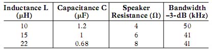
LC Filter Design To save cost and PCB area, most Class D amplifier LC filters use a second-order low-pass design. Figure 3 shows a differential second-order LC filter. The speaker is used to attenuate the natural resonance of the circuit. Although the speaker impedance sometimes approximates a simple resistance, the actual impedance is more complex and may include significant reactive components. To get the best filter design, design engineers should always strive to use accurate speaker models.
A common filter design choice is to minimize filter response degradation to achieve the lowest bandwidth at the highest audio frequency required. If the required drop is less than 1 dB for frequencies up to 20 kHz, a typical filter is required to have a 40 kHz Butterworth response (to achieve a maximum flat passband). For common speaker impedances and standard L and C values, the table below gives the nominal component values ​​and their corresponding approximate Butterworth responses:
If the design does not include speaker feedback, the speaker THD is sensitive to the linearity of the LC filter components.
Inductor Design Considerations: Important factors in designing or selecting an inductor include the current rating and shape of the core, and the line resistance.
Rated current: The rated current of the selected core should be greater than the maximum current of the desired amplifier. The reason is that if the current exceeds the rated current threshold and the current density is too high, many inductor cores will magnetically saturate, causing a sharp decrease in inductance, which is undesirable.
The inductor is formed by pulling a wire around the core. If there are a lot of wires, the resistance associated with the length of the total wire is very important. Since the resistor is connected in series between the half bridge and the speaker, some output power is consumed. If the resistance is too high, you should use a thicker wire or a magnetic core of other metals that requires less wire to provide the required inductance.
Finally, don't forget that the shape of the inductor used will also affect EMI, as mentioned above.
System Costs What are the important factors that affect the overall cost of an audio system using a Class D amplifier? How can we minimize costs?
The active components of a Class D amplifier are the switching output stage and the modulator. The cost of constructing this circuit is roughly the same as that of an analog linear amplifier. The tradeoff that really needs to be considered is the other components of the system.
The low power consumption of Class D amplifiers saves on the cost of the heat sink (and PCB area), such as heat sinks or fans. Class D integrated circuit amplifiers can be packaged in smaller and lower cost than analog linear amplifiers. When driving a digital audio source, an analog linear amplifier requires a digital-to-analog converter (DAC) to convert the audio signal into an analog signal. This is also required for Class D amplifiers that process analog inputs, but the DAC function is effectively integrated for Class D amplifiers with digital inputs.
On the other hand, the main cost disadvantage of class D amplifiers is the LC filter. The components of the LC filter, especially the inductors, take up PCB area and increase cost. In high power amplifiers, the overall system cost of a Class D amplifier is still competitive because the significant cost savings in the heat sink can offset the cost of the LC filter. However, in low cost, low power applications, the cost of the inductor is high. In very rare cases, such as low cost amplifiers for cellular phones, the cost of an amplifier IC may be lower than the total cost of the LC filter. Even considering the cost considerations, the PCB area occupied by the LC filter is a problem in small applications.
To meet these considerations, the LC filter is sometimes completely eliminated to use a filterless amplifier design. This saves cost and PCB area, although the benefits of a low-pass filter are lost. Without a filter, the increase in EMI and high frequency power consumption would be unacceptable unless the speaker was inductive and very close to the amplifier, the current loop area was the smallest, and the power level remained low. Although this design is often employed in portable applications, such as cellular telephones, it is not suitable for high power systems, such as home audio.
Another approach is to minimize the number of LC filter components required for each audio channel. This can be achieved by using a single-ended half-bridge output stage that requires half the number of inductors and capacitors in a differential full-bridge circuit. However, if the half-bridge output stage requires a bipolar supply, the cost associated with generating a negative supply can be prohibitive unless the negative supply already has some other purpose, or the amplifier has enough audio channels to share the negative supply cost. In addition, the half bridge can be powered from a single supply, but this reduces output power and often requires the use of a large DC blocking capacitor.
Fiber Fast Connector,Fiber Quick Connector,Fast Connect Fiber Connectors,Fiber Optic Quick Connector
Ningbo Fengwei Communication Technology Co., Ltd , https://www.fengweicommunication.com