
RFID technology is a non-contact automatic identification technology that performs non-contact two-way data communication through wireless radio frequency to identify targets and obtain relevant data. The RFID system usually consists of three parts: an electronic tag, a reader/writer, and an antenna. The reader operates the electronic tag and feeds back the obtained electronic tag information to the PC. With its unique advantages, radio frequency identification technology is gradually being widely used in production, logistics, transportation, anti-counterfeiting, tracking and military. According to different working frequency bands, RFID systems can be classified into low frequency, high frequency, ultra high frequency and microwave. At present, most RFID systems are low-frequency and high-frequency systems, but the RFID system in the UHF band has the advantages of long operating distance, fast communication speed, low cost and small size, and is more suitable for future logistics and supply chain applications. Although the development of RFID UHF technology is relatively mature, there are already some standards, and the price of labels has also decreased. However, RFID UHF readers have become larger, more complicated and more expensive. It will consume more energy and produce hundreds of components. However, the design here uses a highly integrated R1000 that solves these problems, reducing complexity and production costs in chip design, and enabling manufacturers to create smaller, more innovative readers. Open up new areas of RFID applications.
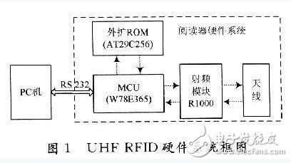
1 reader hardware structure designThe design uses the W78E465 as the main control module and the IntelR1000 transceiver as the RF module. The design can be used as a handheld terminal and connected to the host computer using the RS 232 serial communication module and the level shifting interface MAX232. The system hardware principle is shown in Figure 1.
@5xe" o:preferrelaTIve=â€t†o:spt=â€75†coordsize=â€21600,21600â€
@5xe†o:preferrelaTIve=“t†o:spt=“75†coordsize=“21600, 21600†1.1 Master Module
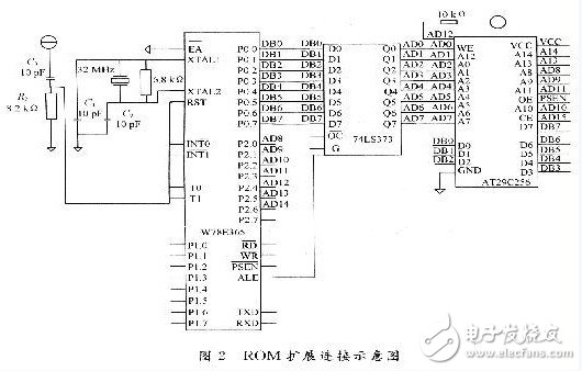
The W78E365 is a low-power 8-bit microcontroller with an ISP-capable FLASH EPROM for firmware upgrades. Its instruction set is fully compatible with the standard 8052 instruction set. W78E365 includes 64 KB of main ROM, 4 KB of auxiliary FLASH EPROM, 256 B of on-chip RAM; 4 8-bit bidirectional, bit-addressable I/O ports; an additional 4-bit I/O port P4; 16-bit timer/counter and 1 serial port. These peripherals are supported by an interrupt system with 9 interrupt sources and 4 levels of interrupt capability. For user-friendly programming and verification, the ROM included in the W78E365 allows for electrical programming and electrical reading and writing. Once the code is determined, the user can protect the code.
The internal ROM of the W78E365 is only 64 KB, and the memory is too small. Therefore, the AT29C256 is used as the external ROM. The line connection is shown in Figure 2.
1.2 transceiver module
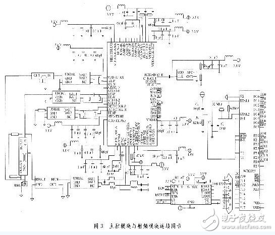
The RF module uses an Intel R1000 transceiver. The R1000 includes an energy amplifier that allows the tag to be encoded and read at close range or within 2 m, depending on the antenna used by the reader. With an additional external energy amplifier, the R1000 reader can read and write up to 10 m. The R1000 must be connected to a separate microprocessor that converts the raw data generated by the R1000 digital information processor into an EPc or 18000-6c format with an operating frequency of 860 to 960 MHz and a total of 56 references. The foot is made of 0.18μm SiGe BiCMOs advanced technology, the volume is only 8 mm & TImes; 8 mm, the power consumption is only about 1.5 w, and it has high integration.
The connection between R1000 and W78E365 is shown in Figure 3. The RF signal enters the bridge through the antenna, and the output signal is divided into two paths. One signal passes through the band-pass filter and the unbalanced to balanced conversion enters the RF input port of the R1000. The other signal is unbalanced to balanced and converted into the local input of the R1000. After the two signals are demodulated and analog-to-digital converted in the R1000, the digital information is sent to the W78E365. The W78E365 decodes and verifies the received signal, sends the obtained information to the host computer, and encodes and encrypts the R1000 command and sends it to the R1000. These commands are modulated and PAd inside the R1000, and then balanced and unbalanced for conversion and filtering, which is transmitted by the antenna. The clock drive in the digital block comes from the 24 MHz reference frequency generated by the external TCXO. The signal frequency through the ∑-ΔDACS in the system is 24 MHz; the signal frequency through the ∑-Δ ADCS is 48 MHz.
The R1000 integrates a receiver and transmitter. In essence, the receiver is a zero IF receiver. After downconversion, most of the DC is reset and filtered by the AC coupling capacitor. The analog IF filter provides a coarse channel selection. It has programmable bandwidth to meet a wide range of digital pass rates. The filter can be configured as two actual low pass filters or as a complex single phase band pass filter. After filtering, the I, Q signals are converted to digital signals by a digital-to-analog converter. An increase in the automatic IF gain in the filter reduces the dynamic range of the analog to digital converter.
In the R1000, the transmitter supports in-phase quadrature vector modulation and polarization modulation. The former is used for SSB-ASK modulation and inverse amplitude shift keying modulation; the latter is used for DSB-ASK. In both modulation modes, the signal generated by the digital module is converted into an analog signal by a △Δ digital-to-analog converter and a reconstruction filter.
In the SSB-ASK modulation mode, the baseband coded signal generates a composite in-phase signal I and a quadrature signal Q via a Hilbert filter, and converts the I, Q digital signals into analog signals via a ∑-Δ digital-to-analog converter. , enter the analog module, the analog signal is transmitted through the antenna. In the PR-ASK modulation mode, the mixer is used to invert the signal to compensate for the delay of the AM part, and the inverse delay control has a programmable delay, so that the time error of the phase and amplitude of the polarization modulation tends to Minimum value. In the DSB-ASK modulation mode, the baseband coding and pulse signals are also generated by a Hilbert filter to generate a composite I, Q signal. The difference is that the pulse shaping signal is pre-distorted to compensate for the nonlinearity in the amplitude modulation transfer function. This pre-distorted amplitude modulation control signal is converted into an analog signal by a sigma-delta digital-to-analog converter and finally transmitted through an antenna.
Based on power requirements and modulation methods, the R1000 has full power nonlinearity, low power nonlinearity and linear three emission modes. In DSB-ASK modulation mode. The R1000 uses a full power nonlinear emission mode. In order to transmit the maximum transmit power value of the antenna allowed by the R1000 to +30 dBm, a PA must be connected to the R1000. Class-C polarization modulation can improve the power efficiency of the system. In this mode of transmission, only the DSB-ASK modulation mode is effective. The low-power nonlinear transmit mode is similar to the full-power nonlinear transmit mode except that the PA is no longer needed externally. Instead, only the internal lower output power is used, and only DSB-ASK modulation is effective in this mode of transmission. In linear transmit mode, the R1000's PA-out signal is connected to an external linear PA because the SSB-ASK modulation requires a linear PA. It should be pointed out that when a single PA is connected to the R1000, the complexity of the system is increased, but at the same time, the power of the transmitted signal is amplified, the signal transmission distance is further, and the read/write distance of the reader is improved.
1.3 antenna
For the Intel R1000 UHF transceiver, the antenna has two configurations based on different antenna subsystems. The first case is the single antenna mode. In this case, a loop is used to isolate the transmit and receive paths, each having the function of a receiver and a transmitter. The second case is the dual antenna mode. The receiver and transmitter are also connected by separate antennas. Usually, two independent antennas are controlled by one switch, and each antenna has only a receiver function or a transmitter function.
For the single antenna mode, since the reflection coefficient of the antenna is not ideal, the receiving gain cannot be too large and there is a problem of saturation. With the high receiving sensitivity of R1000, it can be matched with the coupling of about -10 dB, depending on the isolation of the whole line; for the dual antenna mode, the antenna is better isolated and the receiving path can use high gain.
The design uses a dual-antenna mode with a rectangular microstrip antenna and a coaxial cable to form the antenna for the reader. The substrate material of the microstrip antenna uses a ceramic substrate having a relatively high dielectric constant and a thickness of 0.635 mm. The antenna has a width of 70.5 mm, a length of 52.689 mm, and a microstrip line width of 0.598 mm. The feed point is selected at the center of the wide side of the antenna. After ADS simulation, the center frequency of the antenna is 915 MHz. In order to reduce the antenna reflection coefficient and achieve a better match, a transmission line with a length of 18.471 mm and a resistance of 50 Ω is connected in series with the antenna, and then a transmission line with a length of 24.678 mm and a resistance of 50 Ω is connected in parallel. . According to ADS simulation optimization, the directivity coefficient of the antenna in the maximum radiation direction is 3.535 at the center frequency of 915 MHz; the efficiency is 40.087%; the gain is 1.417.
2 system software design2.1 main program
If the system works under the supervision of the PC, the master-slave communication mode is between the system and the PC. When the system receives the command from the Pc machine, it enters the initialization state and performs the corresponding work according to the main control program. After processing, send the information to the PC. The main program flow is shown in Figure 4.

2.2 Software Design
The design uses Manchester encoding to represent a binary data message with a 2-bit binary number. The rising edge of the encoded waveform is indicated by 01, corresponding to the data information 0; the falling edge is represented by 10, corresponding to the data information 1. First, the w78E365 is initialized, so that the counter TO works in the 16-bit timer working mode; when T1 works in the timer working mode, the initial values ​​are assigned to T0 and T1, so that:
TLO/1=(Maximum number of times to count) %256
THO/1=(Maximum number of times to count) /256
Then, the sync pulse timing value is one-half code width, and the effective data encoding is half-bit code width timing. Then start the timer T0 to detect the arrival of the sync edge. If the arrival of the synchronization edge is not detected, the detection is continued; if the arrival of the synchronization edge is detected, the port state is started to be read, and the timer T1 is started. When the next hop edge is detected, the number of counters is incremented by 1, and the corresponding port number 1 is encoded as 10, and the corresponding port number 0 is encoded as 01. Then enter the next cycle until the number of counters reaches the code length. According to the above operation, the data can be encoded. In the same way, it is only necessary to perform the reverse operation in the reverse decoding.
The method of multi-byte CRC check is generally a shift method. This method is slower to execute, but it requires less space. Another method is to look up the table method, that is, pre-calculate the possible remainder of multi-bytes to form a remainder table, and directly look up the table without performing Binary division. This is a quick way, but it takes a lot of space. If the standard CRC-16 is used for verification, it needs at least 1 to 2 KB, which is very disadvantageous for the MCU, so the former is selected.
The design uses a stream cipher encryption algorithm to divide the plaintext M into a string and a bit string M=m0, m1,..., mj,... and encrypt it bit by bit: EK(m)=Ek0(m0), Ekl(m1), ..., Ekj(mj), ..., where the key stream is K = k0, k1, ..., kj.... For plaintext encryption, the components corresponding to K and M are respectively modulo 2 added to obtain a ciphertext sequence C. At the receiving end, the legitimate receiver adds a simple modulo 2 to the ciphertext sequence C and the key sequence to recover the original plaintext. The sequence cipher uses a bitstream generator to generate a stream of random binary digits, called a cryptographic bitstream. The cipher bit stream is used directly as a key, and its length is equal to the length of the plaintext message. The stream key generator is constructed with a linear feedback shift register, considering that the bit stream generator is not truly random.
2.3 Anti-collision procedure
The design uses a binary algorithm that is not based on bit collisions to achieve collision avoidance. The anti-collision process is shown in Figure 5.

The specific process is as follows:
(1) Send a Request command to the responder;
(2) Send the Group-select command and the Ungroup-select command to all responders, so that all or part of the responders participate in the conflict determination process:
1 If there is a conflict, the reader sends it. The Fail command gives the selected transponder until there is no conflict;
2 If there is no conflict, the reader sends a Select command to the transponder and selects the transponder.
(3) Send a Data-Read command to the selected transponder:
1 If the information fed back by the transponder is correctly received, the reader sends a Success command to the selected transponder;
2 If the feedback from the transponder is not received correctly, a certain number of Resend commands are sent to the selected transponder. If the number of times exceeds this, it is considered that there is a conflict, and it enters step 1 of step (2).
(3) When the reader/writer reads and writes the information successfully, the reader sends an Unselect command to the selected transponder, so that the transponder enters a completely inactive state and no longer answers the command sent by the reader.
In order to reactivate the transponder, it is necessary to temporarily leave the range of the reader to perform a reset. Through the above procedures, the anti-collision function of the system can be realized.
3 ConclusionDesigned for functional and timing simulation in Modelsire 6.1 and integrated with Altera's Quartus II 6.0 StraTIx EPl SlOF484C5 device. The results show that the algorithm uses 347 registers, which is much less than the number of registers used by bit collision-based algorithms, saving hardware resources. The maximum number of read and write tags is 3 595, the read/write speed is up to 1000 tags per second, and the anti-collision algorithm is nearly 50% efficient. It has higher TDMA signal utilization and average recognition efficiency than traditional algorithms. Support SSB-ASK and DSB-ASK dual modulation mode, with single and dual antenna mode, small size, high integration, can be used as a handheld terminal, and can be plug and play in various environments.
Lcd Display Panel,Flat Panel Monitor,Lcd Touch Screen,Lcd Tv Panel
Huangshan Kaichi Technology Co.,Ltd , https://www.kaichitech.com