
Clayton Cameron is a Senior Field Application Engineer (FAE) at Xilinx in Toronto. He joined Xilinx in 2000 and worked at Xilinx’s office in Ottawa, mainly to support telecom customers. As a field application engineer, Clayton supports customers and helps them solve problems. He likes the diversity of this job and the challenges it encounters on a daily basis. In his spare time, he enjoys fitness and enjoys family life.
In the design process, engineers often need a certain amount of creativity (you may call it digital duct tape) to ensure the successful completion of the design. Over the past eight years, I have witnessed many excellent engineers using this method to do a great job, and the main tool they use is FPGA Editor.
With FPGA Editor, you can look at the finished design and determine whether the design intent was actually implemented at the FPGA fabric level – and this is very much needed for any engineer or field application engineer. Suppose you get the collaborator's design and need to modify it, but their HDL source code is very difficult to understand, or there are no notes or documents at all. Maybe you just want to lock some clock logic, but you don't know the name of the instance or how to lock it in the desired position. Some of the techniques discussed below to probe the FPGA fabric and create command-line patches can help designers meet the ever-increasing deadlines.
FPGA construction survey techniquesWhen Xilinx released a tool for a new FPGA device, the first thing I usually do was open FPGA Editor to explore the internal structure of the FPGA device. To do this, locate the Xilinx → ISE → Accessories menu and click the FPGA Editor icon, or type fpga_editor at the command line. With the graphical user interface open, select New from the File menu. FPGA Editor asks for the design file name and physical constraints file. There is no design file yet, so type in a design file name (for example, test.ncd) and select the device type you want to see. The FPGA Editor will use the same name as the name of the physical constraint file and load a blank design.
Another approach is to compile an ISE® tool suite design example provided with the software and load it into the FPGA Editor to view the FPGA fabric. Loading a design instance can show more detail and make it easier to locate the item of interest.
There are only two things to remember when browsing in the FPGA Editor:
How to use CTRL / Shift shortcuts to zoom in and out.
2. If you use the F11 key to zoom in on the selected item.
A quick way to zoom without using a GUI button is to hold down the Ctrl and Shift keys and use the left and right mouse buttons to zoom in and out. To quickly find any item, select the item in the list window in the upper right corner of the GUI. Once you have located the item you are looking for, press F11. The Array window zooms in on the item.
The FPGA Editor has four main windows: List, World, Array, and Block. The List window shows all active items in the design. Use the drop-down menu at the top of this window to select its contents – the list includes components that have been or have not been used, networks or unrouted networks, and more.
The Global View window (World Windows) always shows the complete FPGA silicon view, which is useful when trying to determine the routing of a network. At the same time, the Array window is a dynamic view of the FPGA fabric and logic. If you double-click on any item in the Array view, the Block view is displayed giving the details of the selected item or logical unit.
With FPGA Editor, you can see the physical implementation of the design and determine whether the design intent was actually implemented at the FPGA fabric level – and this is very much needed for any engineer or field application engineer.
These windows can be copied for easy browsing or editing of designs. In many cases, opening the second Array window is more convenient and works in two different parts of the design. For example, suppose you need to add a wire between the global clock buffer and the trigger at the bottom of the chip. If you display the output of the global clock buffer in an Array window and another Array window shows the trigger clock input, it will be more convenient to do. Otherwise, you must zoom back and forth to locate the two ends of the wire. Obviously this is cumbersome.
On the right side of the FPGA Editor GUI is a set of toolbars consisting of 20 function buttons for design viewing and editing. More function buttons can be added by editing the fpga_editor.ini file in the $XILINX/data directory. When viewing the design, the INFO button should be used at any time. This function will transcribe all the information of the selected project to the Console window. This feature is very convenient, you can mark the data in the console window and copy it to use elsewhere, such as writing UCF constraints.
Once you understand the most basic concepts and operations, you can begin to look at the FPGA fabric. Usually I start with the logic of the clock. This includes digital clock managers (DCMs), phase-locked loops (PLLs), global clock buffers (BUFGs), regional clock buffers (BUFRs), I/O buffers (BUFIOs), and different clock regions. (To list items by letter, click on Type to sort in the LIST window.) Click on a DCM and press F11. The ARRAY window will navigate to the selected DCM and zoom in on it. Continue to click on DCM and observe the Console window at the bottom of the GUI, which will show something similar to the following:
Comp "DCM_BASE_inst_star", site "DCM_ADV_X0Y9", type = DCM_ADV
(RPM grid X73Y202)
This is useful data. Copy and paste the above content into the UCF file and make the following changes to lock this DCM logic:
INST "DCM_BASE_inst_star"
LOC=DCM_ADV_X0Y9;
With this method, almost any project in the FPGA can be locked. Here is another example of a BUFG lock:
Comp "BUFG_inst_star", site "BUFGCTRL_X0Y20", type = BUFG (RPM grid X73Y124)
INST "BUFG_inst_star"
LOC=BUFGCTRL_X0Y20;
Go back to the List window again and mark the same DCM. After double-clicking, the DCM and all settings and parameters will be displayed in the Block view. This is a very powerful feature that can be used for any logic project in the FPGA fabric. If you select a slice and double-click it, you can see how the slice is wired and if a carry chain or local trigger is used.
The block view's button bar contains many other options. It is worth mentioning that the F= button button, whose function is to display the complete configuration of the items used in the slice. For example, if you use a LUT6 and a trigger, pressing the F= button will give the LUT's boolean agenda and trigger configuration mode.
Reading Xilinx user guides is one thing, and exploring all logic, switches, and parameters from a view that expands on a computer screen is another matter. Once you are familiar with the FPGA fabric and all resources, the help you get when writing and validating your design will be surprising.
Record the generated patch script in the design flow
When the user edits the design in the GUI environment, FPGA Editor can record user actions. The user can not only save the record action flow, but can also reuse the recorded script later and repeat it. This feature is especially useful when you cannot change the RTL, but you need to modify the design during the design process. Assume that the design uses a third-party IP or Xilinx encryption IP, which includes a global clock and a DCM to generate a clock called interface_clk. Then assume that there is a problem with the ASIC to which the interface is connected and cannot receive data on the rising edge of the pre-defined interface_clk. How to correct this problem?
Of course, you can change the PCB, replace the problematic ASIC, or have a third-party IP team modify the clock output logic to provide a 90 degree phase-shifted interface_clk. All these solutions are time consuming and costly. A simpler recommendation is to use the FPGA Editor to record the modification actions and make the necessary changes to the interface_clk logic to provide the correct clock phase for the ASIC in question. Once you have the relevant modified FPGA Editor script, you can play back the edit steps recorded by these command-line scripts, and you can continue your FPGA design process as normal. After the problematic ASIC is repaired, you only need to remove the FPGA Editor script from the build script, and the interface_clk will resume its normal behavior.
To manually edit a design, you first need to turn on read/write permissions in the FPGA Editor. Click File → Main ProperTIes in the menu bar. Under this menu, you can adjust the edit mode (from No logic Change to Read/Write). Click Apply and you are now ready to edit the design. In the next step using FPGA Editor to record all changes to the design, simply click Tools → Scripts → Begin Recording from the menu bar. The FPGA Editor will prompt for a script name (such as patch.scr). After you enter the script name, you can make the necessary changes to the design.
Running a Design Rule Check (DRC) in a design to see if there is a red flag for a rule conflict is a good way. In my design example, there are 14 warnings, but they can all be ignored. Next we will need to locate the DCM used by interface_clk and create another clock called DCM_clk90_out for this DCM's 90 degree phase shift output. This requires using a global clock routing resource to connect the clock to the BUFG. To add a BUFG, first find an unused BUFG location in the FPGA fabric, right-click and select Add. The tool then prompts you to name the BUFG (clk90_bufg) and determine its type: BUFG (see Figure 1).
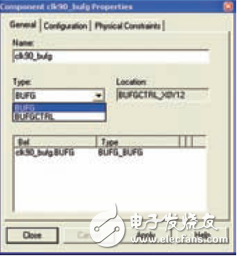
Figure 1: The Properties window allows the user to configure and name the selected logical project
Create a new BUFG, you need to connect its input and output to the appropriate location. In this example, the 90 degree phase shift output of the DCM will drive the BUFG. In the window Array1, click on the 90° attenuator on the DCM. In the window Array2, click on the input attenuator of the BUFG and hold down the Ctrl key to connect. Then release the Ctrl key, click the right mouse button and select Add. The tool prompts you to enter a name for the new network connection. This connects DCM and BUFG together via the new network (see Figure 2).
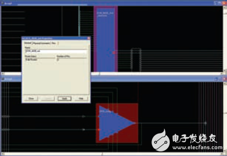
Figure 2: When manually routing in two logical projects, as shown by the red triangle, source and target can be easily selected using two Array windows
The output of clk90_bufg is to replace the clock on the IOB driven by the original interface_clk. To remove the IOB from the original clock domain, locate the IOB, mark the clock input attenuator, and press the Delete key to remove the connection. So we can connect the new clk90_bufg clock here to complete the entire patch. To connect the output of BUFG (clk90_bufg), hold down the Ctrl key, annotate the fader at the output of BUFG in window Array2 and select the clock input for the IOB in the Array1 window. Release the Ctrl key, click the right mouse button to display the options menu and select Add. In this way, the connection between the BUFG output and the IOB is finally completed, and the IOB is used to drive the new interface of the downstream ASIC. The interface_clk90 clock can be used to correctly capture the transmitted data.
This completes the ASIC patch. Now rerun the Design Rule (DRC) Inspector to make sure that no new errors have been introduced. Click Tools →DRC →Run in the menu bar.
When the script is complete and there are no errors, you can go back to the menu and select Tool → Script → End Recording. This will stop and shut down the script logging process and you can reuse this script the next time you need this ASIC patch. A good idea is to open the script file in a text editor and remove all GUI Post and Unpost commands. These commands are not necessary, and keeping them also makes the script difficult to read. The following text is the script of our ASCI patch. As mentioned earlier, the content is very straightforward and easy to read.
Unselect -all
Setattr main edit-mode Read-Write
Add -s "BUFGCTRL_X0Y28" comp
Clk90_bufg ;
Setattr comp clk90_bufg type BUFG
Unselect -all
Select pin 'BUFGCTRL_X0Y28.I0'
Select pin 'DCM_ADV_X0Y11.CLK90'
Add
Post attr net $NET_0
Setattr net $NET_0 name
DCM_clk90_out
Unselect -all
Select pin 'OLOGIC_X0Y2.CLK'
Delete
Unselect -all
Select pin 'ILOGIC_X0Y3.CLK'
Delete
Unselect -all
Select pin 'ILOGIC_X0Y3.CLK'
Select pin 'OLOGIC_X0Y2.CLK'
Select pin 'BUFGCTRL_X0Y28.O'
Add
Post attr net $NET_1
Setattr net $NET_1 name
Clk90_bufg_out
Unselect -all
Drc
Save -w design "patch.ncd"
"patch.pcf"
Exit
End
Take a closer look at the script and see if you can tell which action to take in the corresponding GUI.
It is important that this script can be played back from the GUI (under the menu bar Tool →Scripts →Playback) or on the command line. To add a patch to the build script, just add the following command:
Fpga_edline yourdesign.ncd
Yourdesign.pcf -p yourscript.scr
This command should be executed after the place and route (PAR) is completed, ie after the NCD and PCF files are completed.
FPGA Editor is really a powerful user tool, although not everyone wants or needs to use it in the design process. But when you need some special treatment or need to break the rules in some places to make the design more powerful, no other tool can provide such powerful capabilities as the FPGA Editor. Your FAE can show you its capabilities, show how FPGA Editor can help you complete design debugging and verification, and of course include breakthroughs in the rules.
T Copper Tube Terminals,Non-Insulated Pin-Shaped Naked Terminal,Copper Cable Lugs Terminals,Insulated Fork Cable Spade Terminal
Taixing Longyi Terminals Co.,Ltd. , https://www.longyicopperlugs.com