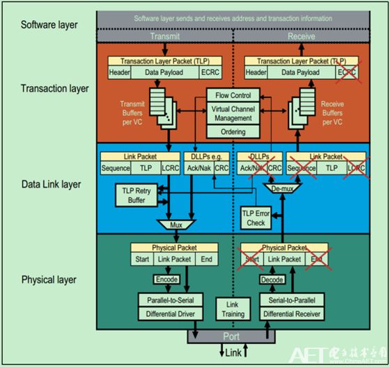
First of all, look back at the PCIe Layer Structure diagram that I've seen many times before:

The physical layer in PCIe mainly performs coding and decoding (8b/10b for Gen1 & Gen2, 128b/130b for Gen3 and later), scrambling and descrambling, serial-to-parallel conversion, differential transmission and reception, and link training. The link training is mainly achieved through the physical layer package Ordered Sets.
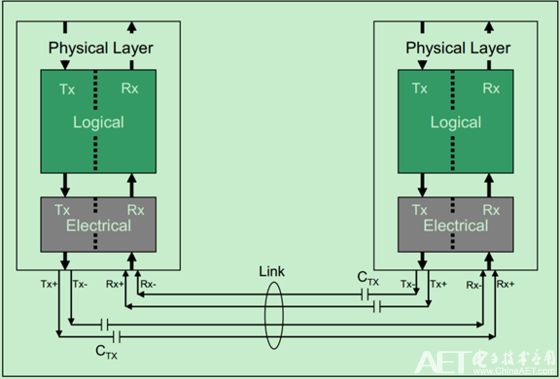
The PCIe Spec divides the physical layer into two parts—the logic sublayer and the electrical sublayer, as shown in the following figure:

As shown in the above figure, the PCIe physical layer implements a pair of transmit and receive differential pairs, so full duplex communication can be achieved. It should be noted that the PCIe Spec only stipulates the functions, performance and parameters that the physical layer needs to implement. However, there is no clear explanation on how to implement these. In other words, vendors can design the physical layer of PCIe based on their own needs and actual conditions. The following will use Mindshare's book to briefly introduce the physical layer logic of PCIe. It may differ from the physical layer implementation of other vendors' devices, but the design goals and the final functions are basically the same.
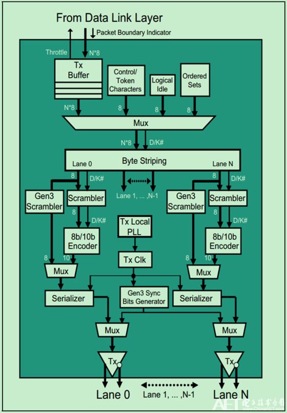
The structure of the sender part of the physical layer logic sublayer is shown below:

Prior to 8b/10b encoding, Mux inserts some content from the data link layer, such as control characters and data characters used to label packet boundaries or Ordered Sets. In order to distinguish these characters, Mux corresponds to the previous D/K# bit (Data or Kontrol).
Note: The figure also includes some implementations of Gen3, but only Gen1 & Gen2 will be introduced here, and Gen3 will not be introduced. If you are interested, you can read Mindshare's book or refer to PCIe Gen3 Spec.
Byte Striping distributes parallel data from Mux to each Lane according to certain rules (more on this later). Scrambler, 8b/10b encoding, Serializer followed by differential transmission pairs are then performed.
Scrambler is based on Pesudo-Random XOR. Since it is a pseudo-random code, as long as the sender and receiver use the same algorithm and seed, the receiver can easily Recover data. However, if the sender and the receiver end up with inconsistent beats for some reason, an error will occur at this time, and Gen1 and Gen2 scrambler will be periodically reset.
Note: The principle and role of 8b/10b are described in my previous post. So the next article will not repeat these contents, but will briefly introduce the 8b/10b implementation details and points in PCIe.
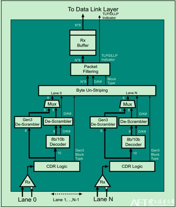
The structure diagram of the receiving end part of the logical layer of the physical layer is as follows:

Since PCIe uses an Embeded Clock (with 8b/10b) mechanism, the receiving end first recovers the clock signal from the data stream when receiving it. This is achieved through the CDR logic. As shown in the above figure, the logic of the receiving end is basically the opposite operation corresponding to the sending end. This is not covered in detail here.
Ic Linear,Linear Amplifiers Video Amps Modules,Ic Integrated Circuit Linear,Ics Linear Comparators
Shenzhen Kaixuanye Technology Co., Ltd. , https://www.iconlinekxys.com
