Hello, everyone, it's time to study everyday. Today we come to chat about clock synchronization in asynchronous circuits.
Since we talked about clock synchronization, what is clock synchronization? First of all, let's find out.
The clock is the reference of all signals in the digital circuit. No clock or clock signal processing is inappropriate. It will affect the performance and even the function of the system. So under normal circumstances, we use the same clock source in the same design. For each clock, you need to select different processing methods according to different situations and synchronize all the clocks. The following describes the clock synchronization methods in several situations.
************************************************** ************************************************** **************************************************
First, when there are multiple clocks in the same digital circuit, and there is one clock (assuming SysClk), the rate is more than twice that of other clocks.
This situation is the simplest, we must synchronize the other clocks in the interface part, and process it as the clock signal synchronized with SysClk. The benefits of this approach are:
1. Facilitate the internal timing of the circuit;
2. The boundary condition between clocks is only processed in the interface circuit.
The general clock synchronization method is shown in the figure below. 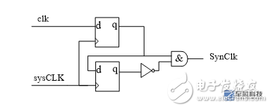
In essence, the synchronous processing method of clock sampling is a rising edge extraction circuit. After the rising edge extraction and output information carries the information of the system clock, it is beneficial to ensure the reliability and portability of the circuit.
************************************************** ************************************************** **************************************************
Second, when all clocks in the system do not have a clock rate equal to twice the other clock frequency, that is, if the clock rates in the system are almost the same
This time cannot satisfy the sampling theorem, so in the interface part other clocks and data must be isolated through the FIFO, and other clock information is converted into an allowable signal synchronized with the system clock. For example, in a high-speed data acquisition system, the acquisition clock of AD is often relatively high, which is more than half of the system clock. At this time, synchronization processing cannot satisfy the timing design.
************************************************** ************************************************** **************************************************
Third, there is data sampling between multiple clocks in the system
The situation as shown in the figure below. The clk1 and clk2 come from different clock sources. The circuit may appear in the same chip, or it may appear in different chips, but all have the same danger. Because of the different clock sources, for the registers reg2 and reg3, at the same time, it is highly probable that one considers the reg1 output to be "1" and the other to be "0", which inevitably results in a circuit result error. 
For this kind of circuit, we must add a flip-flop after reg1, sample it with the clock edge of clk2, and then use the output of this flip-flop to output the combination logic into reg2 and reg3, as shown in the figure below. 
************************************************** ************************************************** *********************
Fourth, multi-level clock or multi-level clock network processing
Due to clock set-up and retention time constraints, FPGA design should try to avoid using multiple clock networks or minimize the number of clocks. Therefore, when FPGAs verify ASIC chips, we must simplify the clock network because FPGAs Internal clock resources are not as permeable and flexible as ASICs. The following figure shows an example of a dangerous multi-stage clock. The input to the multiplexer is divided by 2 by clk and clk. The clock is output by the multiplexer controlled by the SEL pin. In both clocks, the logic is “ At 1â€, when the state of SEL changes, there is a static risk competition phenomenon. 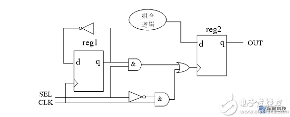
Therefore, in order to ensure the normal operation of the circuit, it needs to be modified. The circuit after modification is shown in the figure below. 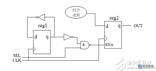
Talk to you today, everyone, continue to cheer!
SMP series Rack-mounted DC Power Supplies are economical, MOSFETs-based, high switching speed, high power density DC power supplies with output power covering 300W ~ 6KW, and maximum voltage up to 800VDC.
Compared with IGBT-based DC switching power supplies, MOSFET-based switching power supplies have a higher switching frequency, making this series Rack DC power supplies can use smaller semiconductor devices and LC filter units while ensuring low ripple, high precision, and fast response characteristics of the Power Supplies DC output. Which gives more space to use a smaller chassis size at the same output power, resulting the high-power density feature of this series Rack Mounted DC power supplies.
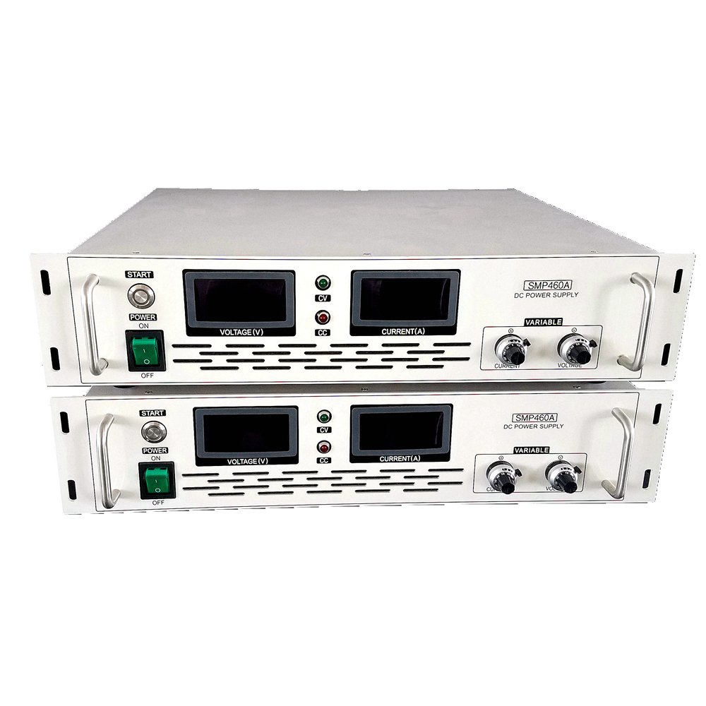
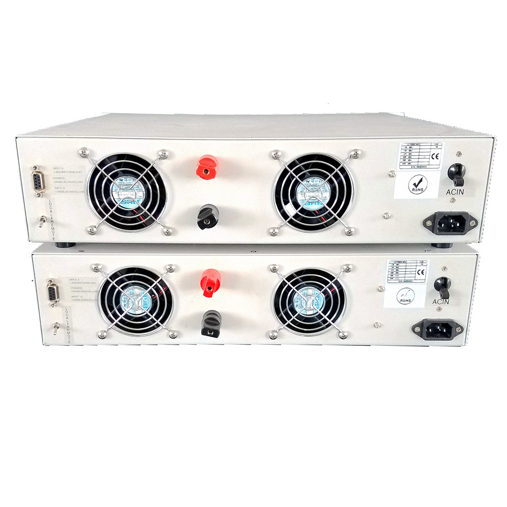
Rack-mounted DC Power Supplies, Rack Mounted DC Power Supplies, DC Rack Power Supplies, Rack Switching Power Supplies, Rack Mount DC Power Supplies
Yangzhou IdealTek Electronics Co., Ltd. , https://www.idealtekpower.com
