
Minimize ringing of the boost converter switch node
Description of the problem
The circuit diagram in Figure 1 (Boost Boost Power Supply) shows the critical loop of the boost converter consisting of parasitic inductance and capacitance. The inductor and capacitor are labeled with the LPAR (parasitic inductance) and CPAR (parasitic capacitance) labels, respectively. The node where the two switches meet the inductance of the switching converter is called a switching node. Parasitic inductance and capacitance typically create mutual inductance and cause the voltage on the switching node to oscillate within the range of 200 MHz+. If the amplitude of the ringing is greater than the absolute maximum value of the rated voltage of the low side switch, the switch will be damaged. In addition, conducted radiation and/or electromagnetic interference (EMI) generated by ringing can also cause problems with adjacent ICs.
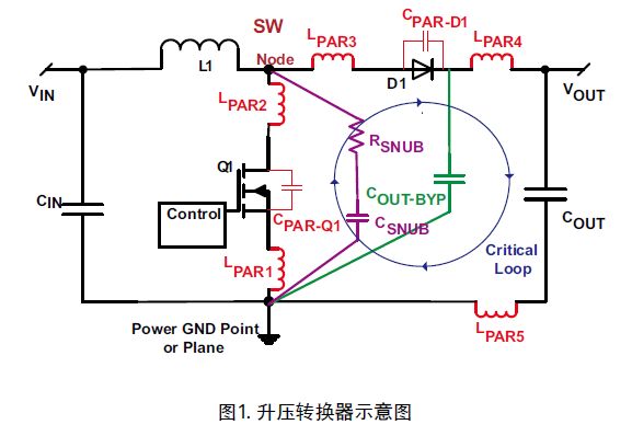
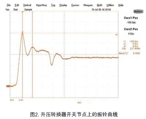
Figure 2 shows the measured curve on the boost converter switching node with a time scale of 5 ns/div. The oscilloscope and oscilloscope probe used for the measurement has a bandwidth of at least 500 MHz, which is approximately twice the estimated 200 MHz ringing frequency. The ground loop of the oscilloscope probe is minimized to avoid distortion of the measurement results caused by inductive pick-up. Since VIN = 3.3 V and VOUT = 5 V, the peak voltage of the switching node should not be greater than VOUT + VDIODE ≈ 5.7 V, but the peak amplitude of the ringing at the switching node is 9.8 V, which may damage the low side switch.
In terms of design, power supply designers have multiple ways to minimize ringing. If a controller is used, designers should use both FETs and diodes with minimal parasitic capacitance and minimize the distance between the two switches and inductors through on-board routing, minimizing LPAR2 and LPAR3. In addition, designers can minimize LPAR1 by reducing the distance between the FET supply pin and the power ground or ground plane. LPAR4 and LPAR5 will also be minimized by placing the large output capacitor as close as possible to the cathode of the diode and the ground supply. The high frequency bypass capacitor (COUT-BYP) between the output value (0.01 mF – 2.2 mF) and the ground supply minimizes ringing. It is also recommended to connect a high frequency bypass capacitor [COUT-BYP] of 0.01 mF – 2.2 mF between the output and the power ground.
Due to board size limitations or internal CPAR#, LPAR1, LPAR2, and LPAR3 with integrated FET power ICs, improved onboard routing is not always possible, so a snubber is required—by RSNUB and CSNUB Composition, from the switch node to the power ground. The snubber circuit is an energy absorbing circuit for eliminating voltage spurs caused by parasitic inductance of the circuit when the switch is closed. When the switch is closed, the snubber circuit provides an alternate ground path for the current flowing through the parasitic inductance of the circuit, thereby suppressing voltage transients and reducing subsequent ringing on parasitic capacitance.
The remainder of the application report walks through how to determine the size of the snubber circuit components to suppress ringing without significantly reducing the rise time of the switch turn-off or reducing overall efficiency.
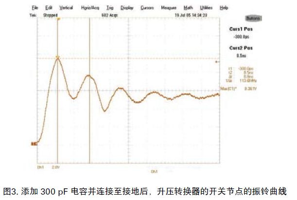
After determining the ringing frequency (fINIT = 217 MHz) caused by parasitic inductance [LΣPAR#] (total parasitic power) and parasitic capacitance [CΣPAR#] (total parasitic capacitance) (measurement waveform shown in Figure 2) As shown), connecting the appropriate capacitor [CADD] between the switch node and ground reduces the ringing frequency to 1â„2. As shown in Figure 3, after adding a 300 pF capacitor, the ringing frequency is 113 MHz.
The resonant frequency of the LC circuit is inversely proportional to the square root of the LC product, and the current total circuit capacitance [CΣPAR# + CADD] is four times its initial value [or CΣPAR# = CADD/3]. This is the minimum capacitance value for CSNUB. The total parasitic inductance that causes ringing can be calculated as follows:

After finishing,

In this example, LΣPAR# is 5.4nH. Finally, the optimum snubber resistance is the characteristic impedance of the original parasitic capacitance [CΣPAR# = CADD/3 = 100 pF] and the stray inductance [LΣPAR#= 5.4 nH]:
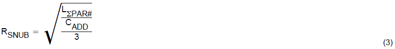
It can be seen from Equation 3 that RSNUB = 7.3Ω and 10Ω after rounding off. Set the value of CSNUB to 330pF, which is greater than the next standard value calculated by CADD. Then set RSNUB to 10Ω, which is connected to ground by the switch node. At this time, take the second measured waveform on the switch node, as shown in Figure 4.
Shown.
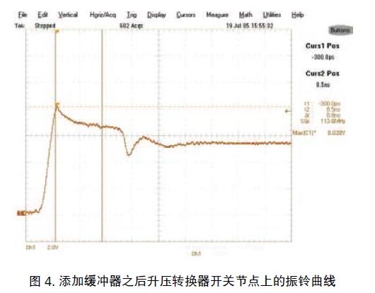
Obviously, the ringing is now basically eliminated, the peak amplitude of the ringing is reduced by 1.8V, now 8V, which is equivalent to a 20% reduction, and the conversion trip time is only shortened by 2ns. The designer can greatly increase the CSNUB value until the transition node angle begins to bend (ie, at Q = 1, the L∑PAR#, CSNUB, and RSNUB circuits are effectively suppressed). However, as the CSNUB value increases, the energy absorbed by the snubber circuit also increases, so the power consumption of the RSNUB also increases accordingly, while reducing the efficiency of the boost converter. The power consumption of RSNUB can be calculated by the following formula: PSNUB = 1/2CSNUB × VPK2 × fSW, where VPK is the reduced peak amplitude and FSW is the switching frequency of the boost converter. Designers must ensure that the RSNUB package is large enough to achieve the above power consumption. In general, the next standard value needs to be greater than the value required to halve the oscillation frequency (1/2 [CADD]). Select CSNUB on this standard value so that the peak amplitude can be reduced by about 20%, while the peak efficiency is reduced. The reduction is not very obvious.
There are similar technical articles on the network that use RC to eliminate the ringing of the secondary diode of the flyback switching power supply. The method is similar.
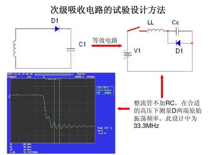
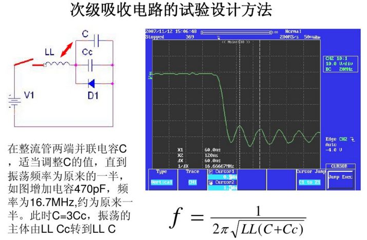
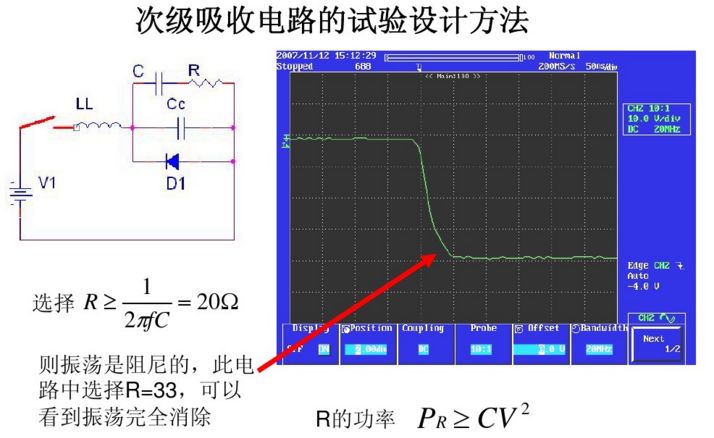
Use RC to eliminate the ringing of the secondary diode of the flyback switching power supply
to sum up
This method has been proved by experiments to reduce or even eliminate ringing. Engineers must first control the power source when designing the switching power supply. Otherwise, the absorption of the addition is very large and the loss is particularly large.
1. Select a MOS or diode with a small parasitic capacitance.
2. When switching the power supply board, try to shorten the distance of the oscillation circuit.
3. Pay special attention to the RC method to eliminate the premise of ringing: the range that must be lost or the amount of heat that can be accepted.
With the improvement of people's quality of life, people's lifestyles have also become varied. Different kinds of recreational products are starting to appear in people's lives, such as electronic cigarettes. The emergence of e-cigarettes represents a part of young people's thinking and means that electronic products are beginning to show a trend towards diversity.
simply replace the pods. The Pod system uses an integrated pod rather than a tank for higher nicotine strength and provides low power traction. the Pod system is rechargeable and has a longer life and higher battery capacity than disposable electronic cigarettes.
Our company Pod system has a built-in 380mAh battery and a USB charging port on the bottom. In comparison, the Pod system has a built-in battery of only 180mAh, but the Pod system charges much faster.
Our electronic cigarettes are of rechargeable construction. The first time you use the charger to charge, it is recommended to use up the remaining power before filling up, this is to ensure the performance of the battery.
Vape Pod System Oem,Vape Pod Oem,Close Pod Oem,Thc Pod Disposable
Shenzhen MASON VAP Technology Co., Ltd. , https://www.cbdvapefactory.com