In a variety of different situations, one needs to transfer large amounts of data from one device to another without errors. For applications where the distance between devices is close, you can choose between PCIE (typical distance is 15 ~ 30 cm) or USB (maximum transmission distance 5 m). For remote distances, you can choose RS232, RS485, Ethernet and other transmission media, and on this basis, through the upper layer protocol to ensure data reliability. The upper layer protocol usually uses the error detection retransmission mechanism to achieve reliable data transmission, such as TFTP, TCP/IP, SCTP, and reliable UDP. These protocols must rely on more complex CPU operations and memory copies to achieve reliable data transfer. For example, under Linux, each time a TCP/IP protocol sends a packet, the CPU needs to execute about 14 000 instructions [1]. Therefore, the operating frequency of the CPU, the read and write speed of the memory, and the hardware I/O bandwidth all affect the speed of the TCP/IP. The TCP performance tests on some embedded systems are shown in Table 1.
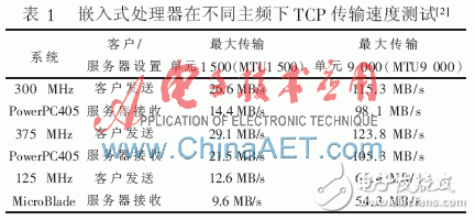
The stronger the CPU processing power, the higher the TCP transmission speed. At the same time, when the maximum transmission unit is 9 000 B (that is, the frequency of the MTU1 500 packet is increased by 6 times and the packet processing frequency is decreased by 6 times), the transmission speed is greatly improved. This also explains the impact of CPU processing power on TCP transmission speed from the side.
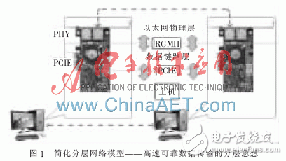
In point-to-point transmission and LAN transmission, there is often no need for a perfect routing mechanism and flow control, but a reliable means of data transmission is also required. The traditional TCP protocol relies on the characteristics of CPU operations, which limits the transmission speed and is unstable due to changes in CPU load [2]. Considering the improvement of transmission efficiency and the reliance on CPU, a high-speed and reliable data transmission method based on hardware is proposed to free the CPU from frequent protocol operations. The method can implement a reliable data transmission protocol on the hardware by writing FPGA logic on the basis of the physical layer communication link provided by the Gigabit Ethernet PHY, and then provide the data to the computer system using an interface such as PCIE. The system structure is shown in Figure 1.
There are many ways to ensure reliability during data transmission, such as error correction code, information feedback, and error detection retransmission mechanism. Selecting retransmission is one of the implementation methods of error retransmission. Compared with waiting for retransmission and retransmission retransmission, it has high efficiency and is widely used. For example, in a TCP/IP network, the principle of error detection retransmission mechanism is used. However, the TCP protocol includes more complex flow control mechanisms and congestion control mechanisms, which are designed to cope with heterogeneous, large-scale complex network environments. In the application of point-to-point transmission, or in a LAN with clear tasks and simple topology, complex routing mechanism and flow control are not needed, so that the widely used error detection retransmission mechanism can be simplified, so that the reliability protocol can be implemented by hardware. . As shown in Figure 2, the process of reliable data transmission is summarized as follows:

(1) The data to be sent is packed at the transmitting end, and the necessary identification information and verification information are added, and stored in the buffer of the transmitting end;
(2) After the Ethernet channel is available, the data packet is sent to the receiver through the Gigabit Ethernet;
(3) After receiving the data packet, the receiver verifies the content, and after confirming that the data is correct, the identification information is fed back to the sender through the ACK data packet;
(4) The sender's buffer receives the identification information and confirms that the data has arrived safely at the receiver, clearing the buffer and waiting to send the next data packet;
(5) If the sender does not receive the ACK feedback with the corresponding identification information within the set time, it will re-send, and the retransmission will report an error if it exceeds a certain number of times.
The verification information is selected to use CRC32 compatible with Ethernet, and the coding redundancy is low (0.26%). It can be foreseen that in the case of general bit error rate (1 & TImes; 10-10), this method can achieve high-speed reliable transmission [4].
Realizing the reliable transmission in hardware mode will greatly reduce the dependence of the sender and the receiver on the CPU resources in the protocol operation, which is quite different from the TCP protocol. As shown in Figure 3, compared to the TCP protocol, the hardware protocol greatly simplifies the data flow when receiving data.
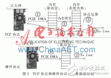
TCP data stream:
(1) The network card receives Ethernet data and writes it to the host computer memory through DMA in PCIE, and triggers an interrupt;
(2) The network packet memory copy enters the OS protocol layer;
(3) protocol operation on the network packet, checking packet header information and CRC check, etc.;
(4) Sending an ACK packet after determining that it is correct;
(5) Provide valid data to upper-level users.
Data flow of the hardware protocol:
(1) The device card FPGA verifies the correctness of the data and spontaneously generates an ACK response packet, and writes the valid data to the host computer memory through the PCIE in a DMA manner, and optionally triggers an interrupt or polls;
(2) The driver layer directly provides data to the user.
The sending process is the opposite of the receiving process, and the situation is similar and will not be described again. It can be seen that the hardware protocol realized by FPGA saves the upper computer software protocol operation and memory copy, directly provides effective data to the upper layer user, improves the efficiency and speed of data transmission, greatly reduces the CPU computing load, and saves the Frequent interruptions in the CPU, resulting in stable, high-speed, reliable data transmission independent of CPU performance. This is difficult to achieve with software protocol optimization.
PCIE interface device card with Xilinx Spartan 6 FPGA and Broadcom Gigabit Ethernet PHY chip. FPGA is the core of the device. The PCIE interface module and the Ethernet interface module are deployed on the FPGA, and the internal logic is designed to realize reliable transmission of data.
2.2 FPGA logic module designThe logic design of the FPGA needs to ensure smooth data flow and interconnection of various modules. A hardware algorithm is used to implement packet packing of data and a response handshake mechanism between nodes to ensure that each data packet arrives at the target device correctly and without error. The internal logic structure of the FPGA is shown in Figure 4. The reliable transmission of data is implemented under the state machine control in the Tx and Rx modules. The Ethernet module is the TriMode Ethernet MAC Core of Xilinx, which provides various rates (10). /100/1 000 M) support for Ethernet PHY. The InterConnect module in the logical core area provides a dynamically configurable interconnect between multiple ports, thus supporting possible network topologies. The PCIE module provides the host computer with access to the data and command channels of the FPGA.
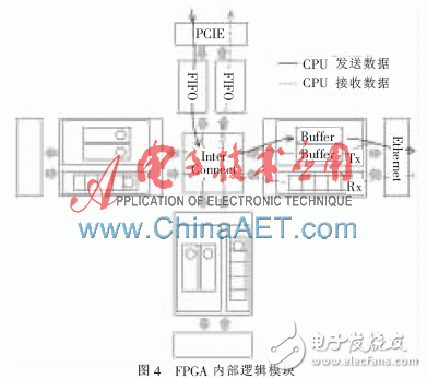
Description of each module of the FPGA:
(1) PCIE, using Xilinx's s6_pcie: 2.4 Logic Core [5]. Two user address spaces are opened, one for accessing the internal state control registers and the other for accessing FPGA data.
(2) InterConnect, under the control of internal registers, interconnects each Ethernet port and the host computer data port according to certain rules, and can perform forwarding between designated ports and transceiving operations of specific ports. And the paradigm style is adopted in verilog coding to facilitate multi-port expansion. In this way, with the cooperation of the upper computer control software, flexible forwarding between multiple ports can be realized, so that the data transmission network can be conveniently set up. The InterConnect data bit width can be flexibly configured and can be configured to be 16 bits wide for Gigabit applications. This module includes other modules inside the FPGA with a clock frequency of 75 MHz.
(3) Tx module, the forwarding data of other ports or the transmission data of the host computer is transmitted to the Tx module via InterConnect, and temporarily stored in a certain Buffer in the data packet unit under the logical scheduling of the Tx module. Each Buffer has its own state machine control. After the data packet is ready in the Buffer, it will be sent to the Ethernet module under the logical scheduling of the Tx module, and the corresponding Buffer state machine is in the state of waiting for ACK. After the counter expires, the retransmission is triggered. If the retransmission is still a certain number of times, there is still no correct ACK response and an error is reported. Multiple Buffers can be parameterized in each Tx module, and the channel utilization efficiency can be greatly improved by the cooperation of multiple Buffers.
(4) Rx module, the internal logic maintains a FIFO-like storage structure. Whenever a data frame is received, the data is temporarily stored in the RAM by accumulating the write pointer, and the destination/source address, frame type, serial number, and the like of the current frame are recorded under the control of the state machine. If it is an ACK frame, the corresponding frame identification information is transmitted to the Tx module; if it is a frame that needs to be received, the memory data is indicated to be valid after the frame is received, and the data valid signal causes the module to be forwarded or the CPU receiving FIFO to read the frame. The Ethernet port of Rx and Tx has a data bit width of 8 bits and an interface clock frequency of 125 MHz.
(5) Ethernet module, using Xilinx's tri_mode_eth_mac: 4.6 Logic Core [6]. The module provides CRC32 encoding and verification, provides support for different rate Ethernet, and provides a uniform data interface to internal logic. 3 System performance test In order to test system performance as completely as possible, it is tested from both logic simulation and actual measurement.
Logic simulation is the simulation prediction of the behavior of FPGA logic using the Xilinx ISim simulator.
The advantage of the simulation test is that the test preparation is simple and the test method is flexible; the disadvantage is that only the logic part of the FPGA can be simulated, and other hardware cannot be simulated.
Considering that the core of the data transmission system is on the FGPA, and through comparison with the measured data, the logic simulation can reflect the system performance to a large extent. The test is a point-to-point transmission between two nodes.
(1) Fixed frame length 1 024 B Test result: bandwidth utilization efficiency is 96.4%, and data transmission speed is 120.5 MB/s.
(2) Random frame length test result: the data transmission speed is 99.4 MB/s, and the bandwidth utilization efficiency is 79.5%.
The simulated waveform is shown in Figure 5. The rgmii_txen_A signal indicates that there is a gap in the channel utilization in this case. This is because the frame length suddenly becomes longer and it is necessary to wait for internal data to be written to the Buffer. This special case can be solved by increasing the number of Tx_buffers.

(3) Artificially added error test results: the data transmission speed is 106.7 MB/s, and the bandwidth utilization efficiency is 85.3%.
The test frame length is 1 024 B. The FPGA is randomly added with a bit error on the transmit port. The test adds a bit error rate of 0.000 76%. In general, the bit error rate is very low (an average bit error causes a packet to be retransmitted). The waiting and retransmission overhead caused by a single bit error is fixed, so the relationship between the change value of the transmission speed and the bit error rate can be approximated as a proportional relationship (? x: transmission rate ratio change; ? station e: bit error rate ):: x = k? stationed in e.
During the test, the error rate was artificially added. The e = 0.000 76%, the x = -13.8 MB / s, and the k = -1.82 & TImes; 106 MB / s. It is estimated that, under normal circumstances (ie, bit error rate 1 & TImes; 10-10), the transmission speed changes? Station x = -1.82 106 MB / s & TImes; 10-10, -18.2 KB / s, the transmission bandwidth is still close 120.5 MB/s.
To test point-to-point transmission between two nodes, two data nodes are required. Node A generates test data, and Node B receives and verifies the test data, and sends it to the PC through DMA in PCIE. The PC-side software checks and counts 100 s of transmitted data and receives 11 742 592 frames for a total of 12.024 GB of data. Test results: the data transmission speed is 120.2 MB/s; the bandwidth utilization efficiency is 96.2%, which is basically the same as the simulation result (96.4%).
3.3 Conclusion According to the test results, the hardware protocol can effectively perform reliable data transmission. In the actual test situation and the expected bit error rate, the transmission speed of sequential transmission of large blocks of data can reach 96% of the Gigabit Ethernet limit bandwidth of 125 MB/s, that is, 120 MB/s. This data is basically the same as the performance of the TCP protocol on the PowerPC405 system with the MTU 9 000 jumbo frame setting (average consideration of reception and transmission), and much higher than the performance of the MTU 1 500 setting. The TCP protocol can be exchanged for higher speeds at low processing frequencies, which means that the transmission speed of the software protocol is greatly affected by CPU operations and is prone to fluctuations. A stable high data rate is the advantage of a hardware protocol.
The reliable transmission of data is a topic of general interest. Based on the existing mature Ethernet technology, this paper uses FPGA hardware to realize high-speed and reliable data transmission. Compared to the complex TCP software protocol, the use of hardware protocols can effectively reduce the CPU load and thus obtain a stable high-speed data transmission rate. The hardware platform described in this article supports the expansion of multiple Ethernet ports. The configurable forwarding function between the ports in the node enables flexible routing under the control of the onboard MCU. In this way, multiple nodes can form a data transmission network, thus providing a feasible solution for network applications such as high-speed data acquisition networks and local area network transmission.
Our company can provide many kinds of high quality vehicle Alarm Speakers,with the advantages of novel appearance, it has clear sound quality, waterproof, corrosion resistance, and good sealing performance.
All electro-acoustic parameters have reached the leading level of similar products, and are widely used in special products police Dept. Fire Dept. Ambulance and fixed places for alarm matching use so on ! it can match with with our all siren products to work !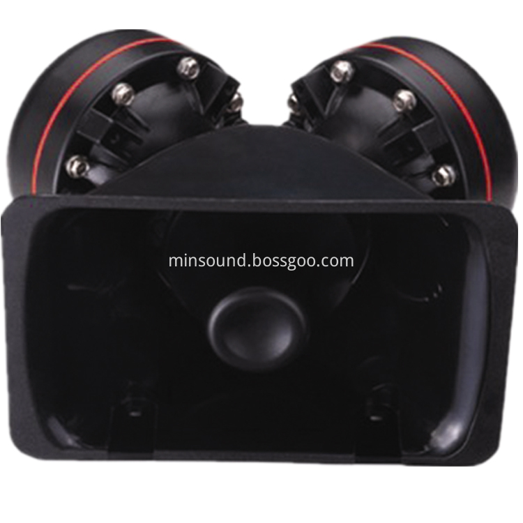

Alarm Speakers,Emergency sirens,Emergency Siren Speakers,Warning Sirens,siren speakers
Taixing Minsheng Electronic Co.,Ltd. , https://www.ms-speakers.com
