3 Buttons Garage Door Automatic Brazil Peccinin Compatible 433.92mhz Remote
Encode Available
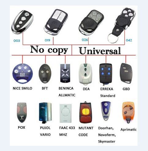
compatable brand remote controls same functions as originalÂ
fixed codeÂ
Learning code, chip EV1527
Rolling code: chip HCS301
Duplicator code/ bluetooth code/ clone code/ universal code
Frequency support
315MHZ, 433.92MHZ, 310MHZ, 350MHZ, 330MHZ, 336MHZ, more
Specification
|
2017 Mini Wireless Auto Remote Control Duplicator Adjustable Frequency 433.92 MHz Garage Learning Code Copy Remote Controller   wireless remote control for car alarm,auto alarm,motorcycle alarm,led light,wireless romote control for warehouse door,carbarn door and gate door,smart key,civil security as house security,commercial security,industrial area by fixed code learning code rolling code and other codes. With low consumption but high efficiency, it will be more and more important to human life Â
 |
 | ||||||||||||||||||||||
| Â | Â | ||||||||||||||||||||||
| Â | Â | ||||||||||||||||||||||
| Â | Â | ||||||||||||||||||||||
| Â | Â | ||||||||||||||||||||||
| Â | Â | ||||||||||||||||||||||
| Â | Â | ||||||||||||||||||||||
| Â | Â |
Photo
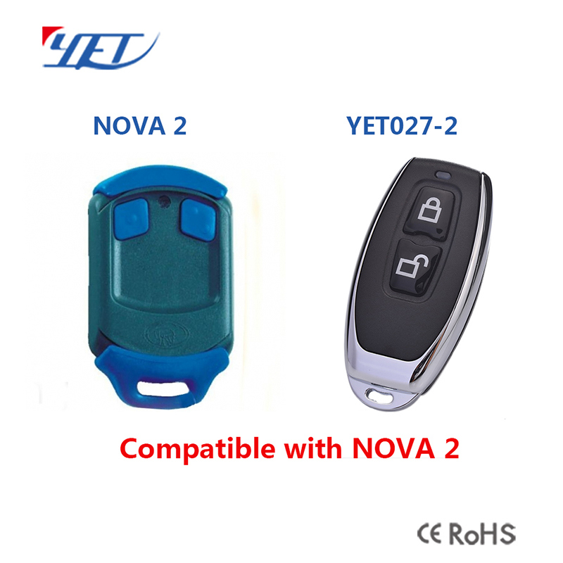
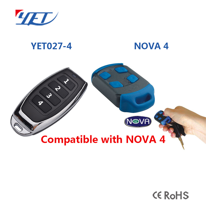
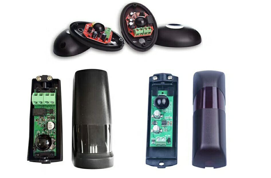
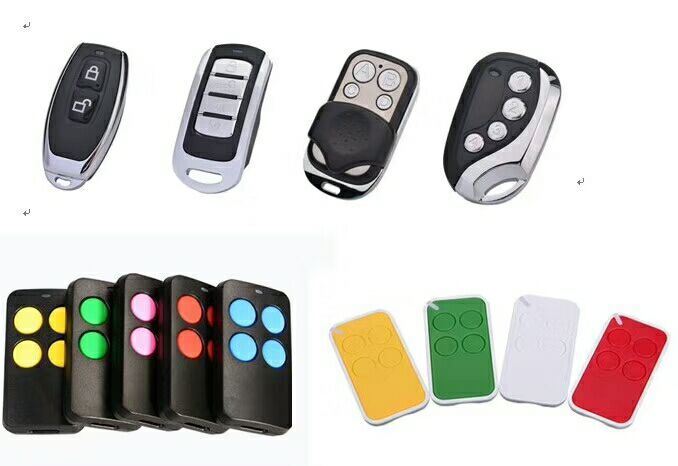
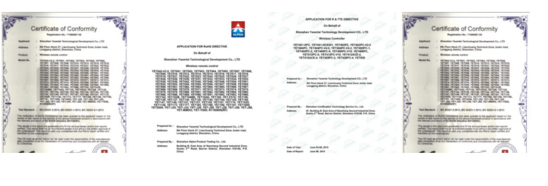
Certifications CE & Rohs
Â
Delivery
1-2 days for sample, 7-15 days for bulk order.
About package:
Poly Bag, Blister, Paper Box, according to customer's requirements...
Â
About Shipping:
Â
DHL, FEDEX, UPS... according to customer's requirement.
Accept OEM, ODM service. About product, 2 years guarantee  for our customer. Any questions, do not hesitate to contact us.Â
FAQ
1. How to know what frequency of my transmitter
Please open the case and found the frequency saw on circuit board, it's surface will be marked with 433.92 or others. Just send this info to us if you are not sure of it.
2. How to pay?
We accept T/T , west union, paypal , L/c.
3. Quarantee
1 years for all products since the day you ordered.
4. Is the product with battery?
Yes.Â
Via In Pad PCB
What is Via In Pad? In shortly,via in pad is the via holes are at the SMD pad.The vias are very small,usually under 0.3mm.Why and how? First is there is no enough space to layout,you have to put the vias and holes closer even together.Second it helps thermal management and for high frequency boards,it may help improve signals.
Because the SMD pads are for SMD components loading,so the solder can not flow to inner layer or the other side when assemble.That is the most important for via in pad board.
How PCB manufacturers like us to do via in pad board? We will fill all vias with non-conductive epoxy and plate copper over it ,so the vias are flat same as others. Many PCB factories are unable to do such capability.
The key technology is how we fill vias and guarantee there is no any solder (surface finishing) in the holes.
Filled via in pad is a way to achieve intermediate density with an intermediate cost compared to using blind/buried vias. Some of the key advantages associated with using the via in pad technology are:
.Fan out fine pitch (less than .75mm) BGAs
.Meets closely packed placement requirements
.Better thermal management
.Overcomes high speed design issues and constraints i.e. low inductance
.No via plugging is required at component locations
.Provides a flat, coplanar surface for component attachment
Via in big pads are not a big problem.but for BGA,that is technology.As BGA pads are very small,10mil or 12mil,and there is no enough space.Manufacturing is not easy as other boards.
Via In Pad PCB
Via In Pad PCB,6Layer Via In Pad PCB,Touch Pad PCB,Via In Pad
Storm Circuit Technology Ltd , http://www.stormpcb.com
