
Design analysis and implementation of multi-chip TS101S loading guide
0 Preface
The ADSP-TS101S digital signal processor is a static superscalar processor with extremely high performance in the TIgerSHARC series launched by American Analog Devices. The processor has been structurally optimized for large signal processing tasks and communication applications, so it has a very wide memory bandwidth and dual arithmetic module f supports 32 bit floating point and 8, 16, 32, 64 bit fixed-point processing), The clock frequency inside the chip can reach 300 MHz at the fastest. The static superscalar structure enables the ADSP-TS101S to execute up to 4 instructions, 24 16-bit fixed-point operations, or 6 floating-point operations per cycle. There are three independent 128-bit data buses inside TS101S. Each one can be connected to one of the three 2 M bit internal memory banks, providing a total of 12 Gbytes / s of internal memory bandwidth.
1 Automatic guidance method
The boot mode of ADSP-TS101S is usually determined by the level of the pin at reset. During reset, if the level of its input pin is low, it is set to EPROM boot mode. For this method, after the signal is invalid, the signal becomes the output signal and serves as the chip selection signal of EPROM; if it is high, the ADSP-TS101S will be in the IDLE state, at which point it will wait for an external host or link To guide. In general, ADSP-TS101S has four boot methods.
1.1 Boot from EPROM
ADSP-TS101S defaults to EPROM loading mode. ADSP-PS101S is generally automatically configured to use external ports and use DMA channel 0 to load 32-bit programs from off-chip 8-bit EPROM to 0x00 to 0xFF of on-chip memory, and automatically pack byte data into 32-bit instructions, its DMA The interrupt vector that has been transferred will be initialized to 0x00000000 after reset. The EPROM memory space is not mapped to the unified storage space of the DSP, that is, after the boot is completed, it has nothing to do with the entire system. The addressing space is limited to a maximum of 16 Mbytes.
1.2 Boot from external host device
Any master device on the shared cluster bus can boot the ADSP-TS101S through an external port and write to its internal memory or automatic DMA.
1.3 Boot from the link port
The DMA of the four receiving links of ADSP-TS101S will be automatically configured to receive 32 bits to 0x00 ~ 0xFF in the internal memory after reset, and the interrupt vector corresponding to the DMA transfer can be initialized to 0x00000000 after reset. Booting from the link port is sometimes called link loading.
1.4 No boot
After reset and start, ADSP-TS101S will generally automatically start execution from somewhere in the storage space, that is, by enabling the interrupt request signal after reset to achieve DSP start.
2 Multi-chip TS101S system program loading hardware design
Using the single-chip FLASH combined with the link port loading method of FS101S can realize the program loading of multiple ADSP-TS101S systems. This method only needs a large-capacity FLASH, without auxiliary logic, can realize multi-ADSP-TS101S system program loading, and multiple ADSP-TS101S can be connected through the link port, thus greatly reducing the system design the complexity.
Figure 1 shows a block diagram of the system loading hardware of a radar signal processor. Among them, the first ADSP-TS101S is connected to FLASH according to the normal FLASH loading mode, and is used to load the rest of the TS101. In addition, the first ADSP-TSl01S also connects the LINK0 and LINK3 ports to DSP2 and DSP4 respectively. Similarly, the LINK2 port of DSP4 and the LINK0 port of DSP2 are also connected to the LINK2 and LINK3 of DSP3, respectively. The interconnection between specific link ports can be flexibly set according to needs. 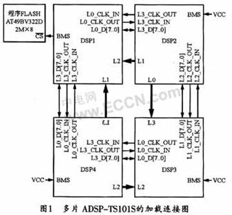
When loading specifically, DSP1 should first load the program through the FLASH program loading method. That is, after the DSP1 program is loaded, the DSP1 reads the second piece from the FLASH again, so that the DSP2 (or DSP4) program passes through the link port. After that, load DSP2 (or DSP4) using the link port loading method. After waiting for DSP2 to load, DSP1 reads the program of DSP3 from FLASH and sends the program of DSP3 to DSP2 through the link port DMA method (or DSP4), and DSP2 (or DSP4), after receiving the third piece of DSP3 program, also loads DSP3 through the link port loading method ... and so on, until all ADSP-TS101S is loaded.
With the multi-ADSP-TS101S system with this structure, the program of each ADSP-TS101S should be placed in different address segments of FLASH separately. The program of the first ADSP-TS101S is stored in the first address of FLASH from 0. The second ADSP-TS101S is stored in the second address space following the first address, and the third ADSP-TS101S is stored in the third address space following the second address ... and so on, just Different ADSP-TS101S programs can be placed in the corresponding address space. But it should be noted that the actual address stored in each ADSP-TS101S program must be a multiple of 16, because the link port of the ADSP-TS10lS must transmit 4 words (4 * 32 bits) each time, and FLASH is 8 bits. So each time the 128-bit program code, that is, 16 FLASH address data will be read. Figure 2 shows the storage of multiple ADSP-TS101S programs in FLASH. 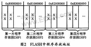
In this design, FLASH chose Atmel's AT49BV322D, and set it to 4 M × 8 mode, therefore, its byte pin needs to be pulled down, the hardware interface circuit between the specific and DSP is shown in Figure 3. 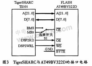
TIgerSHARC processors can support 8-bit, 16-bit, 32-bit, and 64-bit configurations, which brings convenience to different types of external memory interfaces. When the FLASH device is selected to achieve system loading, the TIgerSHARC processor is used to perform a write operation to FLASH, and the data will not be automatically packed into bytes. Therefore, when writing a word to FLASH, this word will be driven to the external bus [31: 0] on. The FLASH memory is only connected to the lower 8 bits of the TIgerSHARC external data bus, so only the lowest byte of human data is written, and the data preparation format is shown in Figure 4. 
3 Automatically guided software design
Since the method of combining EPROM and link port is used to load the multi-DSP program, the link port loading program must be added at the beginning of no DSP program except for the last DSP (DSP3). Under the ldr subdirectory of the VisualDSP ++ installation directory, ADI provides the standard load core file and the corresponding source program (.ASM), and also gives the link description file. Generally, you can directly use the provided standard load core file or simply modify the corresponding source program (modify the current DSP receive link slogan), recompile the link to generate the required load core file.
Because ADSP-TSl01S has three kinds of booting methods (not considering the non-booting method), ADI provides three different loading core files (TS101_prom.dxe, TSl01_link.dxe, TS101_host.dxe). The core ideas and functions of these three programs are completely the same, but because of the different loading ports and methods used, the specific code implementation is slightly different. Based on the above analysis, it can be seen that the reset boot of ADSP-TS101S essentially includes two aspects: one is to add an additional 256-word loading core file at the beginning when generating the loading file; the second is at the end of reset Afterwards, according to the different boot methods, it automatically receives the 256-word code (actually loading the core file) from the corresponding interface to 0x00 ~ 0xFF of the internal storage space, and after completing this reception process, the internal storage space 0x00000000 starts to execute the program (actually it is to load the core file), and finally the core file is loaded to complete the loading of the entire executable program.
TigerSHARC can only continue to load user programs after running the load core code. However, loading the core file does not always occupy 0x00 ~ 0xFF of the internal storage space, because the loading of the core file will automatically complete its overwriting at the end.
This design is composed of four TS101 cascades to form a multiprocessor system. In addition to the first DSP (DSPl) selecting the default EPROM to load, the remaining three DSPs must select LINK to load. At the same time, for the first DSP, the procedure of forwarding DSP2 or DSP4 first is equivalent, because DSP2 and DSP4 themselves are equivalent in this design, both belong to the second level DSP, and DSP1 belongs to the first level. DSP3 belongs to the last level. In the same way, DSP3 can be used as any subsidiary DSP, so it may be the next level of DSP4 (this connection is used in this design). The first TS101 needs to load the second and third level ADSP-TS101S through the link port, and it needs to add the loading program to load the subsequent DSP before the first level application.
Since the program of each DSP is composed of the loading code and the user code, when the first DSP loads the program to the second and third levels, the loading code and the user program should be transmitted separately. Figure 5 shows the program flow chart of the first DSP. 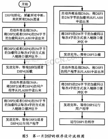
Because DSP3 is loaded as the next-level DSP of DSP4, program code for the third-level DSP to forward the loading code should also be added in DSP4. The program flow chart of the second DSP (DSP4 in this design) loading the third DSP (DSP3 in this design) is shown in Figure 6. 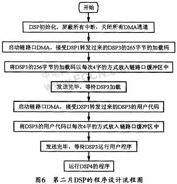
It should be noted that each ADSP-TS101S needs to calculate the length of the subsequent ADSP-TS101S program in advance when loading the program of the subsequent ADSP-TS101S. This value is needed when transmitting user programs. Therefore, if this value is calculated incorrectly, it will cause an error in the ADSP-TS101S program loading.
4 Conclusion
If you do not use SDRAM in the system, you only need to make a few modifications to the standard loading core source program provided by ADI, and then recompile and link to use. And if there is SDRAM in the system, it is necessary to add the initialization of SDRAM at the beginning of the standard loading nuclear source program.
Ningbo Autrends International Trade Co.,Ltd. , https://www.mosvape.com