In today's fast embedded system design, the most popular solution is to integrate application software or soft IP platform in FPGA to simplify the process and accelerate the product launch schedule. For this reason, many companies have introduced their own development platforms and related CPU IP cores. There are two common ones: one is general-purpose CPUs, such as 32-bit and 64-bit general-purpose CPU cores from xilinx and altera; the other is dedicated The most common one is the CPU core of the 51 series single-chip microcomputer, but the current soft cores of the single-chip microcomputer are basically 8051, and there are few other varieties. Moreover, the speed of 8051 is not very fast. In some fast control situations (such as using a single-chip microcomputer as a control component of usb2.0), it appears that the speed is insufficient. The Core8051 launched by the well-known Actel company has a running frequency of only about 40 MHz. This article introduces the design of a very high-speed DS80C320 microcontroller soft core.
DS80C320 single-chip microcomputer is a high-performance single-chip based on the 51 frame introduced by DALLAS.
It has the following advantages:
â… It has an instruction system that is completely consistent with the 51 series, and is fully compatible with all programs developed based on the 51 series;
â…¡, has more complete peripherals than 8051. Compared with 8051 single-chip microcomputer, DS80C320 adds timer 2 and an enhanced serial port, etc.;
Iii. It has better efficiency than 8051; DS80C320 has 4 CLKs per instruction cycle, 8051 has 12 CLKs. This difference is especially obvious when processing simple instructions, such as single-cycle instruction processing, DS80C320 only needs 4 According to statistics from DALLAS, the execution speed of each instruction of DS80C320 is 1.5~3 times that of 8051. For typical applications, the execution speed is also 8051. About 2.5 times.
â…£, the way of reading instructions is more suitable for the characteristics of IP core than 8051; removing the internal ROM of the single-chip microcomputer and reading instructions completely from the outside, this feature is very suitable as a soft core, first of all, the structure is simple, which is conducive to instruction reading Secondly, the pipeline design can break through the limitation of the internal ROM size. Finally, as a feature of FPGA design, even in the 8051 design, the internal ROM block is placed in the ROM resource of the FPGA chip. Instead of this, it is better to put it directly outside. Simplify timing and structure;
2 Overall structure divisionThe figure shows the overall function diagram of the DS80C320 soft core:

Figure 1 DS80C320 functional block diagram
The design of this IP core mainly arranges the functional blocks according to the instruction execution process, and transmits data through the data bus; the dotted line is the CPU core; first is the ROM module, DS80C320 does not have internal ROM, so the function of this module is mainly to analyze from The instruction read from the P port, and by looking up the length of the instruction and the number of cycles, the relevant control signal is calculated and sent to the CPU control module to control the reading of the instruction; at the same time, if the instruction is LCALL or ACALL, you can analyze the sub The program entry address is reported to the PC module to guide the PC to jump correctly; while the ROM module analyzes the instruction, the decoder DECODER is also performing the decoding action. It will analyze three important parameters based on the 8-bit data of the instruction :ALU action type, the operation data source and reading method of the instruction, the storage location and storage method of the instruction result; the first parameter is sent to the ALU module, and the other two are sent to the CPU control module; the CPU control module CPU_CON is The core part of the entire CPU mainly fulfills two functions: read data control before ALU execution, and write-back data control after ALU execution is completed; this module also controls the timing of the entire CPU and monitors the execution of other modules; ALU It is mainly to complete the calculation work; the INteR module is the control module of the interrupt system, and its function mainly completes the effective judgment and sorting of the interrupt request submitted by each interrupt source, generates the interrupt flag and submits the judgment result and the interrupt entry address code to ROM module to instruct the program to jump. It also needs to be responsible for clearing the interrupt flag after the interrupt is completed and restoring the interrupt level before the interrupt; DS80C320 has three timers and two serial ports, of which timer 2 and serial port are not It can be cut if necessary; as for other modules or registers, they exchange data through the data bus under the control of the CPU control module; it can be seen that the idea of ​​this design is to control the execution and timing of the entire CPU by CPU_CON, and control the entire interrupt system with INTER. The register uses the data bus to complete the data exchange, evenly distributed on both sides of the data bus, the structure is clear and simple, and the regular design is also conducive to improving the speed and facilitating the reduction.
3 Some design features 3.1 Timing designIn the DS80C320 MCU data, there is only an introduction to the timing of the external interface, and there is no explanation for the internal signal execution, so it needs to be re-planned. This soft core analyzes the timing of the DS80C320 in detail, and adds pipeline skills according to the black box idea. , The design of its timing is as follows:
For the execution process of ordinary instructions, the internal timing is divided as follows:
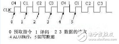
Figure 2 DS80C320 internal timing diagram
This is the execution process of a single-byte single-cycle instruction. The decoding starts on the rising edge of C1 and the length cycle table of this instruction is searched. At the same time, the data bus is the result of the previous instruction that is being written back; the rise of C2 At this time, the control of the data bus and the address bus is returned to the hands of this instruction. At this time, the address bus is used to send the address of the data that needs to be read, and the data bus is ready from sending data to receiving data. This action It is completed by the CPU control module; then on the rising edge of C3, the selected module reads the relevant data according to the address bus and the control bus and sends it to the data bus. In the next clock length, the ALU receives the data, and then At the rising edge of C4, data processing starts. At the same time, the CPU control module changes the content of the address bus and the control bus again, and issues a write signal, prompting the module that started the selected reading to give up control of the data bus, and the selected storage The module analyzes the write type of the result, and prepares to receive the data. After the calculation is completed, the ALU puts the result on the data bus, and waits for the C1 of the next cycle to start writing the result to the relevant location; in short, the design makes full use of the data The resources of the bus and the skills of pipeline design can simplify the operations that originally required 6 timings to 4, and the timings are compact and the speed is fast. At the same time, the idea of ​​distributed processing is adopted, which greatly simplifies the functions of the CPU control module. Issue control signals. The specific module that needs to perform what function is determined by the module itself based on the control signal, which is helpful to avoid the problem of local overheating of the chip caused by too concentrated local functions;
3.2 The design of instruction length periodic tableThe instruction length table is mainly used to control the fetching of instructions and to identify instruction codes and instruction parameters; while the instruction cycle table is mainly used to control the execution time of instructions. These two tables can simplify the control of instruction execution. Generally, this process is performed by the ROM module to look up the table according to the instructions that have been read, and then process and analyze according to the results of the table look-up and the timing situation, and generate a series of control signals and send them to the CPU control module. The main advantage of this is to avoid the CPU. The control module deals with instructions and data, reducing the number of its input and output ports; the design of the instruction length periodic table is closely related to the reading method. This design uses a table built by itself and is divided into two. The processing method is: index ={lsb_3, ir[7:4]}, where the meaning of lsb_3 is: For the lower three bits of the instruction (ir (2 downto 0)), the rule is: 8-F=》7,6-7=》6,0 -5 does not change. The two tables use the same reading method, which can simplify the structure, reduce the search space to 7 bits, and increase the search speed;
3.3 The role of PC transaction codeIn the microcontroller, the PC needs to be constantly changing. Not only all jump instructions need to change the content of the PC, but also interrupt instructions need to complete the stack and push operations of the PC; therefore, in some models, the PC The processing is extremely complicated. Basically, it specifies the changes of the PC in detail for each instruction; this design adopts coding techniques to improve the speed; firstly, analyze the possibility of coding. Although many instructions can change the content of the PC, For the PC, in addition to the normal plus 1 operation, there are only the following ways to change:
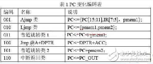
Among them, pmem1 and pmem2 are instruction parameters, which come from the ROM module; PC_OUT is the PC content in the stack.
The remaining problem is who will issue the code. For all jump instructions and interrupt instructions, the jump conditions of each instruction are different, and they need to be judged one by one. This design uses the ALU module cleverly. To process this code, the ALU module also needs to judge the operation when calculating. Therefore, only a small piece of code can be added to complete the function of sending the code; the method of PC coding greatly simplifies the operation of the PC module and makes the program more Regular
3.4 Simulation of bidirectional P portThis is mainly the simulation of the P0 and P2 bidirectional ports; for a typical single-chip microcomputer, the P port is generally bidirectional, but for FPGA design, with the current chip structure, it is impossible to achieve true bidirectional in the FPGA chip. Therefore, as a soft core, the two-way simulation must be handled well; there are several common solutions: one is to directly change the two-way port to two unidirectional ports, which is used for the soft core It is more convenient. This design also provides this method for selection, but this is different from the standard single-chip microcomputer. Therefore, this design also provides an analog two-way port. According to the characteristics of the FPGA design, the direction of the signal line can be changed. There must be a switching process, so you have to carefully analyze the instruction sequence to see if you can handle the switching process in the gap used by the P port; the first is to analyze whether the instruction needs to use the P port, and the more important control signals are translated The RD_LATCH signal sent by the encoder is used to distinguish whether the instruction needs to use the P port, and the control bus information from CPU_CON is used to inform the specific function that the P port needs to complete; if the multiplexing function of the P port is required, Related modules that need to use the P port (such as serial port modules) send request instructions; then the P port analyzes all use requests and arranges different usage conditions according to different usage methods; if two-way switching is required, according to timing and instructions Features to deal with, so as to successfully complete the two-way switching process.
4 Synthesis and verificationUse Altera's Quartus II 4.2 software for synthesis, and use Nios Development Board and Cyclone Edit development boards for board verification; the synthesis results are as follows:
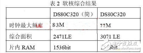
Among them, the previous version is the version without internal serial port; the results of timing simulation verification show that the system can work stably at the above frequency; theoretically, the main frequency converted to 8051 is: 83*2.5=207.5M, which Basically, it can be adapted to most occasions that require microcontroller control; simulation tests mainly use modelsim SE5.8 and quartus4.2 VWF file tests; on-board waveform observation mainly uses Agilent’s 1673G logic analyzer; at the same time, it makes full use of A large number of system-level tests have been performed on the resources of the development board; the program is downloaded to the chip, and the execution waveforms of some instructions are observed using logic analysis:
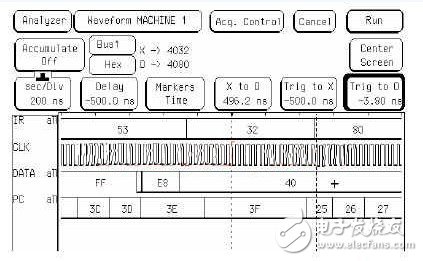
Figure 3 Waveform diagram of interrupt command
This is a waveform diagram of an interrupt return instruction. The instruction code is 32H. It mainly observes the change of PC. After this instruction, the PC changes from 3FH to the address 25H before the interrupt occurs.
5 concluding remarksThis design has the advantages of fast speed, can be cut down, has good reusability and portability, is fully compatible with DS80C320 microcontroller interface, and is convenient to use. In particular, the specially constructed internal framework and timing distribution make its high-speed performance basically the forefront of the current 51 series of soft cores. Therefore, it can be easily applied to FPGA design and embedded system design that require a microcontroller soft core.
ZGAR Aurora 3000 Puffs
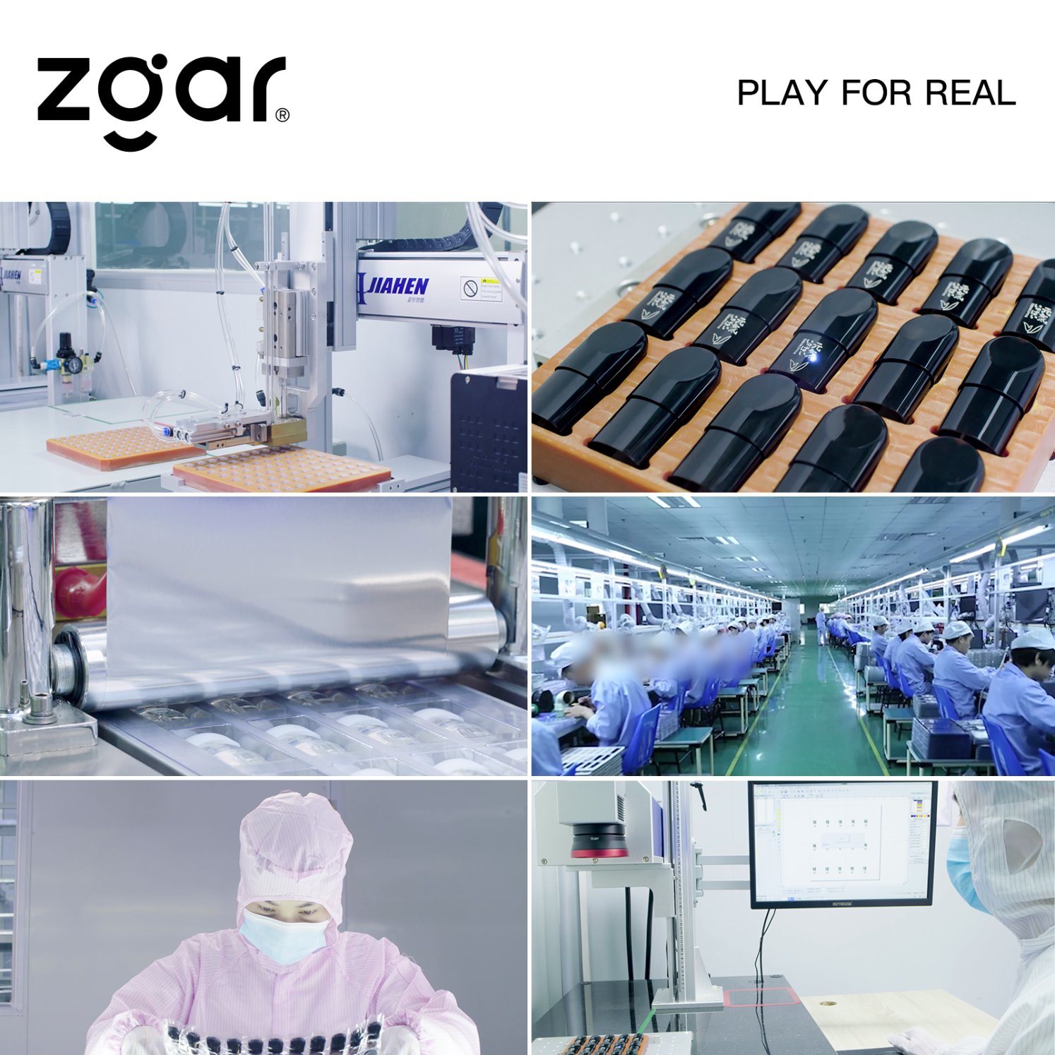
ZGAR electronic cigarette uses high-tech R&D, food grade disposable pod device and high-quality raw material. All package designs are Original IP. Our designer team is from Hong Kong. We have very high requirements for product quality, flavors taste and packaging design. The E-liquid is imported, materials are food grade, and assembly plant is medical-grade dust-free workshops.
Our products include disposable e-cigarettes, rechargeable e-cigarettes, rechargreable disposable vape pen, and various of flavors of cigarette cartridges. From 600puffs to 5000puffs, ZGAR bar Disposable offer high-tech R&D, E-cigarette improves battery capacity, We offer various of flavors and support customization. And printing designs can be customized. We have our own professional team and competitive quotations for any OEM or ODM works.
We supply OEM rechargeable disposable vape pen,OEM disposable electronic cigarette,ODM disposable vape pen,ODM disposable electronic cigarette,OEM/ODM vape pen e-cigarette,OEM/ODM atomizer device.
Aurora 3000 Puffs,ZGAR Aurora 3000 Puffs Pod System Vape,ZGAR Aurora 3000 Puffs Pos Systems Touch Screen,ZGAR Aurora 3000 Puffs Disposable Vape Pod System,3000Puffs Pod Vape System
ZGAR INTERNATIONAL(HK)CO., LIMITED , https://www.szdisposable-vape.com
