Electrostatic discharge (ESD) has existed from the beginning. Our first exposure to ESD is often when we were children. When we touch a metal door handle on a dry winter day, we will feel an electric shock-this is electrostatic discharge. This short-term discomfort is usually not a problem for humans, but even a small amount of ESD may damage sensitive circuits.

Mobile phone designers have always faced the challenge of when and how to solve this natural phenomenon. Why is system-level ESD protection so important? How to improve test models and strategies for system-level ESD protection in mobile devices?
1 ESD model and waveform testing
The human body and clothes can store 500 V to 2,500 V electrostatic charge per day, but humans can only feel 3,000 to 4,000 V ESD pulses. This is much higher than the level of damage to electronic circuits, even if humans cannot detect it.
The designer must solve the ESD problem from many aspects. For the component manufacturer, it is at the end of the design stage and design work. In short, ESD protection requires a multi-level approach.
Generally, integrated circuit (IC) manufacturers design, test, and verify their ICs in accordance with ESD industry standards. This prevents physical damage during IC production or assembly on PC boards. For ESD, the two types of tests that are usually performed include:
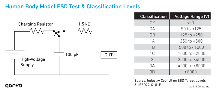
Human body model (HBM). This test simulates an ESD event in which the human body releases the accumulated static electricity through contact with the IC. A charged 100 pF capacitor and a 1.5 kΩ discharge resistor are used for simulation.

Charged device model (CDM). This test simulates the charging and discharging events that occur in production equipment and processes. The equipment gains charge in some friction processes or electrostatic induction processes, and then suddenly comes into contact with a grounded object or surface.

Although device-level testing can help measure the ESD robustness of ICs, system-level testing can measure the protection of electronic devices in the field (ie original equipment manufacturer [OEM] equipment or end products).
In order to better understand the ESD protection required by the final product, the OEM should adopt a system-level ESD approach to design, and then test the final product in accordance with the International Electrotechnical Commission (IEC) ESD standard 61000-4-2. IEC 61000-4-2 is regarded as the industry standard for ESD testing and rating of end products. This test can determine the vulnerability of the system to external ESD events on site.
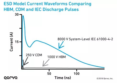
The figure below compares the energy and peak current of the three pulses:
System level IEC 61000-4-2
Device-level HBM
Device-level CDM

The IEC ESD event pulse is obviously stronger, so the equipment in the system is more difficult to pass. Although device-level tests (HBM and CDM) are useful and provide a benchmark for ESD robustness, it is not always possible to determine survivability during system-level IEC testing.
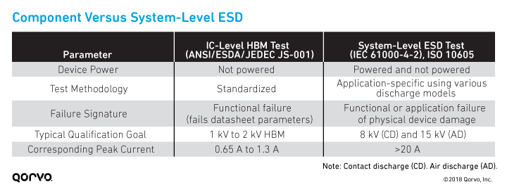
To further demonstrate this concept, the table below shows the difference between component testing and system-level IEC testing. As you can see, the difference is large, and the system stress level is higher. All in all: Compared with equipment-level design, system design must meet more stringent requirements.

2 Insufficient testing
System-level ESD testing during the development phase can be a problem. For example, ESD on test evaluation/incomplete board components is not representative of all situations. The results of these components do not guarantee the final result of the complete system.
Device-level ESD testing (ie, HBM and CDM) aims to produce repeatable and reproducible results suitable for discrete components in the factory through proper ESD control. This is the so-called ESD protected area (EPA). However, these tests are not intended to solve all product-level ESD events outside the scope of the EPA in the real world.
3 The key to product robustness: system-level ESD
On the contrary, the key to ESD robust system design is to consider the impact of ESD in the system. In order to obtain a system-level perspective, designers must understand and solve the following issues:
System-level stress events and their impact on the entire product. Device-level ESD test results can only provide very little information for system ESD design, because they cannot reflect what the electronic device has experienced during an IEC ESD event.
The board-level interactions in the system and the transient behavior of pins that are in contact with the outside of electronic components under ESD stress.
Efficient characterization methods (such as component-level transmission line pulse (TLP) data) are used to analyze the interaction of ICs, boards, and systems.
The system-level ESD protection strategy depends on the physical design, product requirements, and product cost.
4 Best Method: System Efficient ESD Design (SEED)
System Efficient ESD Design (SEED) is a system-level method that considers the transient response of all components in the system. The SEED method also includes the physical influence of the IEC stress applied to the external ports of the PC board on the IC pins.
SEED is a collaborative design method that implements on-board and on-chip ESD protection. With SEED, you can analyze and implement system-level ESD robustness. This method requires a comprehensive understanding of the interaction between external ESD pulses, complete system-level board design, and device pin characteristics during ESD stress events.
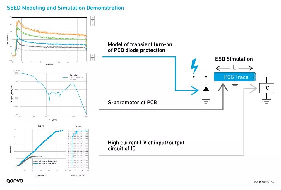
The SEED method is the best method to achieve symmetrical and robust system-level ESD protection. As shown in the figure below, SEED uses the following information to design system-level ESD protection:
Quasi-static TLP current-voltage (IV) curve data
Transient simulation
S parameter PC board data
IC IV circuit measurement

The ESD protection of the PC board is the primary protection, which can prevent physical damage to the IC or the system, and the on-chip protection plays the role of secondary protection. The basic concept of SEED is to prevent damaging ESD pulses from reaching the internal IC pins. Appropriate system-level ESD design can be realized by executing and analyzing ESD system-level simulation.

As we all know, it is very important to implement ESD strategically in mobile phone design. Doing so can shorten the design engineering cycle time, reduce ESD failures and R&D expenses. In the follow-up WeChat, we will discuss ESD protection components and different strategies to reduce the impact of ESD on mobile RF design and explain how to use simulation and modeling to determine system-level ESD protection.
There are many different versions of DIN Connectors. The name of each type comes from the number of pins the connector has (3-pin DIN, 4-pin DIN, etc.) Some of these pin numbers come in different configurations, with the pins arranged differently from one configuration to the next.
DIN cable connector 3-pin, 4-pin, 5-pin, 6-pin, 7-pin, 8-pin degree 180, 216, 240, 262, 270
DIN cables, DIN connector, telephone cable, computer cable, audio cable
ETOP WIREHARNESS LIMITED , https://www.wireharnessetop.com
