A previous article introduced the steps for writing simulation test files:
1. Write test to A module, its test module name is A_tb, for example, original module name is called led, test module name is called led_tb;
2. Copy all input and output ports of the A module, that is, the I/O declarations (input and output signals). Note that this does not include intermediate variables (reg type and wire type signals); change all inputs to reg, output change. For wire;
3. Then copy the port definition part of the A module, including the module name to the end of the semicolon, and instantiate the module;
4. The significance of the test module is the analog input signal, to verify whether the original module's output signal conforms to the code logic. Therefore, in the test module, it is necessary to write an initial block to simulate all the input variables and perform the assignment operation.
5. If there is a clock, it needs to generate a clock signal again;
6. Finally add the time stamp.
This article details how to do it. The example given is an example of selecting a data selector in the previous article. Everyone can do it.
design background:
Test files are especially important in our projects. For example, we need to verify the correctness of your modules. Do you want to verify the validity of your modules? If your project is small, if you compile more than 10 minutes, don't you? Waiting for a stop, if it's possible to modify the test file, so if we can design our test file, then verify our system first. If our logic is correct, we can go to work to see if it is not correct then we We can use the signaltap tool in quartus to capture our signal to verify, which will be explained in our future documents.
Â
Design principle : Â
Our design is a simple two-to-one multiplexer. We write a test file by giving this simple multiplexer and let everyone have a simple understanding of the test.
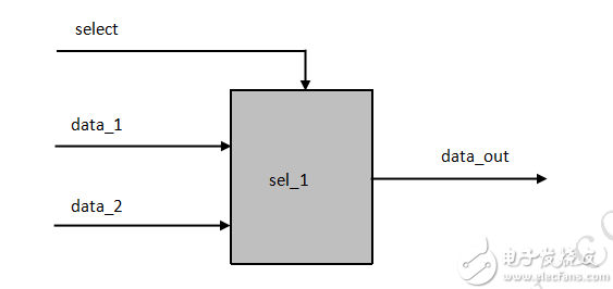
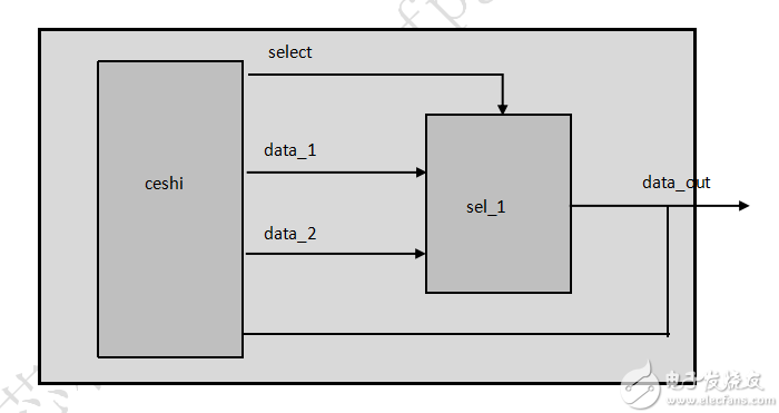
In the architecture we can clearly see the architecture we designed. Our project has 2 input data data_1, data_2, an input select bit select, and an output data_out. In fact, writing tests to this architecture is also motivation. In fact, it is said that white is to write input to it. When it is written well for input, we can not verify its logical relationship in the simulation tool.
Â
Design architecture diagram :
Sel_1 architecture

Overall architecture

Design code :
We write the following code, we look at it, and then we explain to you how to write the test
Modules
0 Â Module sel_1 ( data_1 , data_2 , select , data_out );
1 Â
2 Â Input data_1 , data_2 ; // data input
3 Â Input select ; // select bits
4 Â
5  Output  Reg data_out ; // Output of data
6 Â
7  Always  @  (*)
8 Â Begin
9 Â If ( select ) // If the select bit is high, output data_1
10 data_out = data_1 ;
11 else // If the selection bit is low, output data_2
12 data_out = data_2 ;
13 end
14
15 Â Endmodule Â
Â
Test module
The simple test of the test, the test module input is defined as register reg type, the output is defined as wire type, then add our block initial, plus our instantiation, as follows:
0   `timescale  1ns  /  1ps
1 Â
2   Module  Module Name;    Â
3 Â
4  Reg  An input module;
5  Wire  Output module;
6 Â
7  Initial  Begin
8 Â
9 Â
10
11
12 end
13
Example 14 alias module name (
15 Â Port (Port),
16 Â Port (Port),
17 Â
18 Â );
19 Â
20 Â Endmodule Â
In the test, we also have many systems such as our system task $stop, etc. These are grammatical knowledge, we can buy a suitable book to see, we write for our design incentives are as follows:
Â
0   `timescale  1ns  /  1ps // 1ns in this row defines the unit of time for our test, followed by ps which is the accuracy
1 Â // The timescale in front of English is the meaning of time quantum
2 Â
3 Â Â Module sel_1_tb ; Â Â Â Â / / Module followed by our test name, generally we write module names
4 Â // add _tb, if we write a program to test multiple modules that we will be able to clearly distinguish
5 Â
6 Â Reg data_1 , data_2 ; // Define the input and output of the module
7 Â Reg select ; // The input in the module is defined as a register
8 Â
9 Â wire data_out; // output wire type is defined as a linear
10
11 initial  Begin //initial is a string type that is synthesized in the test.
12 // If you write to the module, it will be reported incorrectly
13 data_1 = Â 0 ; // Then we can define our port and give our port initial value
14 data_2 = Â 0 ;
15 select = Â 0 ;
16
17 # 200 data_1 = Â 1 ; data_2 = Â 0 ; Â Â Â // Delay 200ns to input assignment
18 # 100 select = Â 1 ; // Assignment to selection bit after delay of 200ns
19 # 100 select = Â 0; // After 200ns delay assigned to the selected bit
20
21 # 200 data_1 = Â 0 ; data_2 = Â 1 ;
22 # 100 select = Â 0 ;
23 # 100 select = Â 1 ;
twenty four
25 # 300 Â $stop ; //The $stop system task, which means stop, this is the delay after 300ns , the simulation stops
26 Â End
27 Â Â
28 Â Sel_1 sel_1_dut ( Â Â Â Â Â // The instantiation of the module, and the connection to the port
29 Â . Data_1 (data_1),
30 Â . Data_2 (data_2),
31 Â . select ( select ),
32 Â . Data_out (data_out)
33 Â );
34 Â
35 Â Endmodule Â
Â
In the test, if we use the clock, we can write it like this:
0   `timescale  1ns  /  1ps
1 Â
2   Module  Module Name;    Â
3 Â
4  Reg  An input module;
5  Wire  Output module;
6 Â Reg clk , rst_n ;
7 Â
8  Initial  Begin
9 Â Clk = Â 1 ;
10 rst_n = Â 0 ;
11
12 # 200.1 rst_n = Â 1 ;
13
14 end
15
16 always  # 10 clk =  ~ clk ; //always always, this can be written as a 50M clock
17 // say the delay is 10ns flipping once, that is, a period of 20ns
18
Example 19 alias module name (
20 Â Port (Port),
twenty one  Encoder
Optical Rotary Sensor,Custom Encoder,Optical Encoder 6Mm Shaft,Handwheel Pulse Generator
Jilin Lander Intelligent Technology Co., Ltd , https://www.jilinlandermotor.com
