
Taking advantage of the launch of our NB's i.MXRT series, which is known as the cross-border processor, I think it's fast (remember that Kinetis just came out, I just started writing a series of technical documents at school, this is awkward, fate). In fact, before I published it to AET, I first sent this article to the Amo Forum and tried the test. I received a sentence that made me feel agitated, that is, "FSL is alive again", my answer is "Soul In...", hey, hey, don't say it, let's open it.
Before the official formation of this article, after three versions of modification and optimization, the final bugs were fixed and the known bugs and stability were dare to come up with ugliness. I hope that the majority of AET bloggers will continue to gain some experience. It is also a contribution to the future development of RT1050. It seems that many people are watching the RT series. There are also many third-party design companies and open source projects that are eager to move, so I hope that this brick I will throw can be stimulated in the wide market of RT. A little bit of good jade comes out. . .
At the beginning of the 2018 New Year, I.MXRT105x has been introduced to the market for a while, and it has attracted a lot of interest from customers in the industrial and consumer sectors due to its extremely high cost performance. After all, compared with most of the existing high-priced and low-priced products on the market. "The high-end ARM Cortex-M7 product, RT105x up to 600MHz frequency, extremely rich peripherals and 3 dollars starting position is really the industry's conscience (and the upcoming LQFP package I.MXRT1020 is even more exciting), Of course, this kind of "low price and high allocation" has a price. The internal flash does not need to be connected to the serial SPI Nand/Nor Flash or the parallel Nand/Nor Flash (it seems to have poured cold water on a lot of people.) Hehe), but this news is that some people are happy with some people's worries. For the happy customers, their application code itself can't be installed in the internal Flash. It's better, the province's inner heart is entangled and no longer need to worry about the boss. I urge myself to optimize the code streamlined application all the time to see if I can only use the internal Flash to get it, haha, and the external SPI Flash with a few Mb or tens of Mb is cheaper and upgrade later. Chuo more than, and to worry about customers, bring external Flash startup mode startup configuration complexity, code security issues and the impact on system performance are all potentially thorny issue.
Regarding the code security of external Flash and the impact of external execution on the performance of the entire system, RT105x's Encrypted Boot (HAB) function and 32KB of L1 ICache/DCache can be solved, but this article starts with the RT105x boot configuration problem. After all, if the system is not Boot, other problems are empty talk, huh, huh. In addition, as mentioned above, RT105x supports a lot of startup methods, but personally feel that external serial SPI Flash startup is a compromise for most people. Since the RT105x's official EVK board comes with two serial SPI Nor Flash (one is Cypress's high-performance 8-wire high-speed Hyper Flash).

S26KS512SDPBHI02, one is ISSI's inexpensive 4-wire QSPI Flash IS25WP064AJBLE), so I have a flaw in it. Take the on-board Hyper Flash and QSPI Flash as an example to illustrate the startup process and specificity of serial SPI Nor Flash. Instructions.
Serial SPI Nor Flash startup process 1
When the Boot mode selection switch SW7 on the RT105x EVK is set to the first two shown in Table 1-1 (the other BOOT_CFG pins are pulled down to the ground by default, that is, the OFF state), the system will execute the external through the on-chip FlexSPI interface. The serial SPI Nor Flash is started, its startup address is 0x6000_0000 shown in Table1-2 (if it is started from parallel Nor Flash, the startup address is 0x8000_0000). For the influence of other Boot pins on the startup mode configuration, see RT105x RM. Section 8.6 of the manual, I will not elaborate here.
Table1-1 Typical Startup Mode Settings
| SW7-1 | SW7-2 | SW7-3 | SW7-4 | Startup mode |
| OFF | ON | ON | OFF | Hyper Flash startup |
| OFF | OFF | ON | OFF | QSPI Flash startup |
| ON | OFF | ON | OFF | SD card boot |
Table1-2 Start the relevant address
| Start Address | End Address | Size | Description |
| 0x80000000 | 0xDFFFFFFF | 1.5GB | SEMC external memory interface (SDRAM, parallel NOR Flash, PSRAM, Parallel NAND Flash) |
| 0x60000000 | 0x7F7FFFFF | 504MB | FlexSPI |
| 0x20200000 | 0x2027FFFF | 512KB | OCRAM |
| 0x20000000 | 0x2007FFFF | 512KB | DTCM |
| 0x00000000 | 0x0007FFFF | 512KB | ITCM |
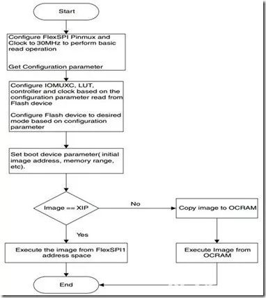
Figure 1 shows the complete SPI Nor Flash startup flow chart. When the on-chip ROM of the RT105x detects the startup mode as the FlexSPI interface, it will configure the complex of the FlexSPI interface pins to be used in this mode according to the configuration information of the Boot Pin. Use the mode and configure the FlexSPI clock to the default low speed 30MHz, then read the first 512 bytes as the external Flash configuration information with 0x6000_0000 as the first address (ie Flash Configuration Parameters, including several lines of SPI Flash, SPI clock) Frequency, LUT lookup table, DDR/SDR mode and Chip/Supup Time for chip select CS pins, see RM8.6.3) and configure the FlexSPI module to meet the characteristics of external Flash. After configuration, RT105x The CPU will read the data and instructions in the AHB bus in the future (although it is still the FlexSPI interface from the outside, but since the LUT lookup table has read the data read command, the CPU can only send the read command through the AHB bus. Trigger the LUT to operate the external Flash, which means that the underlying FlexSPI has been masked internally to the CPU to read the next image with the user. The key information of the IVT (Image Vector Table), Boot Data and DCD (Device configuration data) is shown in Figure 2. The IVT needs to be placed at the fixed offset address of the external Flash (as shown in Figure 3, for Nor Flash. Need to store the offset address of the base address + 4KB, such as 0x60000000+4*1024) for ROM read so that the system knows where the first executable instruction of the user Image is placed and the storage address of BootData and DCD, BootData The first address of the full Image and the size of the entire image are saved, while the DCD contains configuration commands for the ROM to call the configuration internal peripherals to better match the external IC before jumping to the user program entry, generally if the system In the case of external SDRAM, DCD needs to be configured (because sometimes the main program needs to be in the ready state before running, so that the CPU will not make mistakes when copying data or code into SDRAM).

Figure 1 SPI Nor Flash startup process
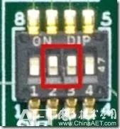
Figure 2 complete Image component
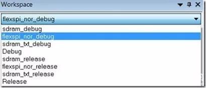
Figure 3 IVT storage address for different storage media
In summary, we can actually conclude that if you want the system to boot properly, the complete image written into the external serial SPI Flash must include five important elements, Flash Configuration Parameters. IVT, Boot Data, DCD and user image, where Flash Configuration Parameters and IVT are stored at fixed addresses, while the latter three are determined by the content of the IVT, either directly compiled or manually added by assistive tools, as long as we The resulting image contains these elements, and the CPU will recognize the image and execute it (not to mention security encryption). So as long as we figure out the basic principle, no matter what method, in the end, we will all go the same way. Here we can safely solve the FlesSPI startup problem of RT105x.
SPI Nor Flash startup configuration method 2
As mentioned earlier, if you want the RT105x to boot normally from the external serial SPI Nor Flash, the image to be programmed must integrate five elements (Flash Configuration Parameters, IVT, Boot Data, DCD and User Image, important things to do. More to say a few times, huh, huh), that specific implementation method I am thinking of nothing more than two, one is to link these elements and application code directly in the compilation link process, and specify these links The address is finally downloaded to the SPI Flash via the IDE's Flashloader. The second is to manually add an information header (the header contains these elements) in front of the compiled bare application code through the auxiliary tool, and then through a separate Download the tool or the ROM bootloader ISP inside the MCU. These two have their own advantages and disadvantages, the former is more suitable for use in the early debugging, so you can directly download and debug online (such as single step, breakpoint, view register and Memory) when editing and modifying the application code in the IDE. Etc.), I believe this is more urgently needed now, but the shortcoming is that the pre-configuration process is slightly more complicated and requires some understanding of the Boot process and the external SPI Flash Spec (of course, these configurations are once and for all, configured once The latter is the configuration that the customer does not need to care about other elements. It only focuses on the development of the user application. After the development is completed, the final image is generated by the auxiliary tool for small batch testing or mass production. The disadvantage is the pre-commissioning. It will be more troublesome. Every time you modify the recompilation and generate the user image, you need to manually add the information header with the auxiliary tool and then download it through the Bootloader to verify it. (I think it is a bit tired.) In this case, the workaround can only be the first one. Debug in RAM, go through this process after you are mature.)
The second method of using auxiliary tools, the official has provided a complete set of toolchain (can be found in the RT105x official home page of the "Flashloader i.MX-RT1050" package) and has the corresponding AN application notes to introduce its specific steps I won't go into details here. This time we will focus on the first method, which is to generate and download and debug the complete image through the configuration of the project in the IDE environment. I will say a few more words here. In fact, this method is not only convenient. Download and debug, the benefits are also quite a lot. First, all the configuration information of these elements are reflected in the application project file in the form of constant C language, which will deepen our understanding of Boot, so if you replace the external SPI Flash can also easily change the adaptation information. The second is that the image file formed in this way will be in the common image format (such as .bin, .hex and .S19), and will be compatible with most of the market. Batch programming of mass production tools for SPI Flash. Ok, no more to say, let's say something awkward, huh, huh, because there are two kinds of Hyper Flash and QSPI Flash onboard, the following explains the configuration methods of these two kinds of Flash in the IDE environment (I use IAR, Keil can refer to the fourth chapter to configure itself, several files need to be added is compatible with IAR, Keil and GCC environments).
Develop a test environment:
Hardware Platform: MIMRT1050-EVK (SCH-29538 REV A1)
Software Package: SDK_2.3.0_EVK-MIMXRT1050 (mcuxpresso.nxp.com)
IDE: IAR_v8.20.1
Debugger: On-Board CMSIS-DAP
2.1 Cypress 1.8v Hyper Flash Boot
The RT105x EVK board is started by Hyper Flash by default, so the hardware does not need to be changed. Just change the SW7 startup mode to the first line of Table1-1 to enable Hyper Flash startup, as shown in Figure 4 below, then we will use SDK2. The hello world in 3 is an example to introduce the specific configuration method. In fact, in the latest SDK2.3, the Keil and MCUXpresso versions already have a sample of hello_world_xip for Hyper Flash, but IAR is not, but this is exactly the same as we have to go through the complete configuration process. A small section of QSPI startup lays the groundwork (there is no QSPI XIP routine in the official routine), after all, most customers are expected to prefer QSPI.
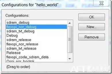
Figure 4 Hyper Flash boot mode
(1) Open the hello world routine \boards\evkmimxrt1050\demo_apps\hello_world\iar of SDK2.3. Under Workspace, you can see that there are 8 configurations by default, including SDRAM debugging, OCRAM debugging and spi nor Flash debugging. The original flexspi_nor_debug configuration has no other elements, so this configuration can be debugged online when the code is downloaded to the external Hyper Flash. However, when the power is restored or the external reset is performed, the system cannot be booted because there is no other. The element information RT1050 cannot be recognized when it is started. Next we create a new configuration based on this configuration and then add files and modify the configuration on the new project configuration, click IAR menu bar Project->Edit Configurations, then select New under the open window, under the new project configuration Start a new name "HyperFlash_bootok", Base on Configuration select the original flexspi_nor_debug to retain the original configuration to the maximum extent, after clicking OK, the current project will enter the newly added HyperFlash_bootok configuration state;

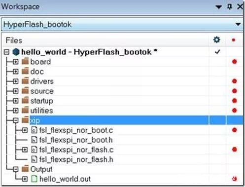
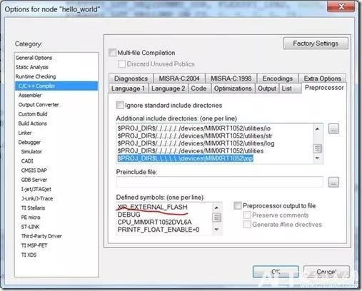
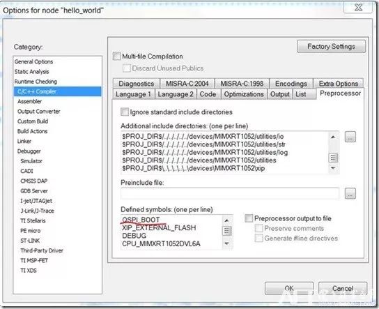
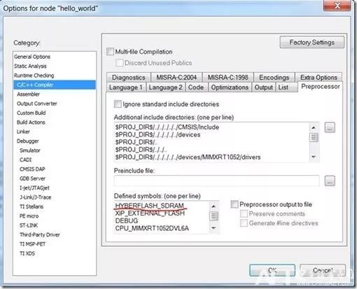
(2) Under this project configuration, add a new group (right-click project -> Add-> Add Group) and name it "xip", then right-click the Group->Add->Add Files and find the root directory \devices\MIMXRT1052 Four files in the \xip path, add the four files to the current project, as shown below, we can open these two .c files to see the four elements except the User Image It is defined in a constant way within the specified segment address, so that after the link is compiled, the element configuration information is assigned to the specified address to be saved on the final Image, and the four files are compatible with IAR, Keil And GCC three compilers can be free to porting, of course, do not forget to add the path of the two header files in the header configuration search path in the project configuration, and if there is no XIP_EXTERNAL_FLASH this macro should be added;
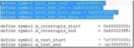
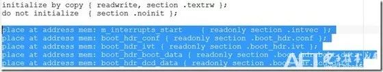
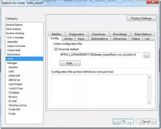
(3) Since the four elements are respectively defined in the specified segment, the default link file in the original project is not defined by these segments (Keil and MCUXpresso are defined because of the xip example. )), so we need to add the definition of these segments and assign the address based on the original link file. We renamed the original link file MIMXRT1052xxxxx_flexspi_nor.icf to MIMXRT1052xxxxx_hyperflash_nor_bootok.icf (the name does not matter), then Open the file, add the definitions and address assignments of these sections as follows (see the compressed package attached to this document for the modified source files), then select the newly modified link file in the project configuration Options->Linker, and finally click OK. ;
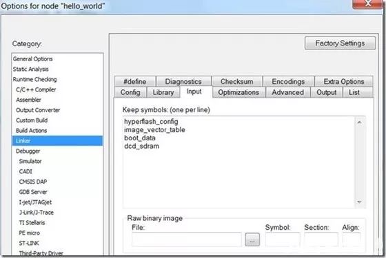
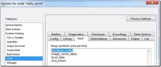
(4) Do not think that this is over, huh, we have said that several important element information is stored in the specified address segment in the form of constants through the link file, but our application project does not call them. At compile time, the compiler will optimize them by default. The final work is not reflected in the Image. The previous work is white, so you need an extra step to tell the compiler to keep these constants to Keep. The specific configuration is as follows: Figure, then click to confirm;
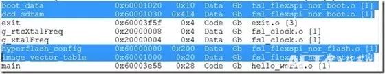
(5) This project configuration is over. We recompile the entire project, and then in the generated .map file, we can see that the following four elements have been correctly assigned to the specified address, so that everything is ready. It’s the difference between IDE IAR’s Flashloader and Dongfeng.
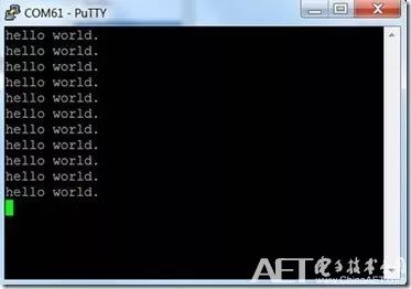
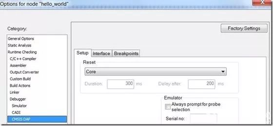
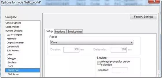
(6) In the version of IAR v8.20.1 or higher, there is already a Flashloader for HyperFlash. We select CMSIS-DAP under the Options->Debugger option, and then the next thing to note is the Options type under the Options->CMSIS-DAP option. Need to choose Core Reset (CMSIS-DAP default Reset mode will lead to breakpoints when debugging, J-link does not have this problem), then click Ok to keep the configuration, and finally start Debug can be perfectly with a few important The configuration data of the element information is downloaded into the external Hyper Flash and enters the Debug mode. Normal single step or breakpoint, and the button reset or re-powering the board can make the RT105x boot normally. Finally, there is a picture with the truth and a serial port. Printed results for "hello world", Enjoy it...

2.2 ISSI 1.8v QSPI Startup
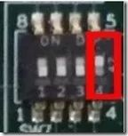
After talking about the startup method of Hyper Flash, let's continue to talk about QSPI startup. Since the Hyper Flash and QSPI clocks, chip selects and some data lines on the board are shared, it is necessary to solder the Hyper Flash when testing the QSPI startup (related to the board hardware design, not soldering will affect the timing, slightly Distressed, after all, Hyper Flash is more expensive and BGA can't be welded down. Of course, if the customer's own design board only has one kind of SPI Nor Flash, then there is no such problem), then the following figure On the 0 ohm resistance welding of DNP, the last special attention is to pull the 4.7k resistor to the power supply Flash_VCC on the 7th and 3rd pins of the QSPI Flash, ie Reset and WP pins. Because I found that there are some models of QSPI Flash, such as the ISSI for the board, the Reset and WP feet are suspended when the system is started, and the QSPI Flash is powered by the single line mode by default, so if Reset and WP are If it is low, QSPI is always in the reset and write protection state, which causes the system RT1050 to fail to read the QSPI information and cause the startup to fail. Therefore, it is necessary to add a pull-up resistor to the two pins to give it a valid high level. I tested the QD and Winbond QSPI. These two legs have pull-up resistors. After the system is started, it is fixed at a high level. There is no problem, but my suggestion is that it is better to add one to the outside to ensure reliability. Will affect the subsequent 4-wire communication. In addition, don't forget that the SW7 boot mode needs to be modified to enable the QSPI Flash boot in the second row of Table1-1, as shown in Figure 5 below:
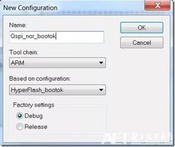
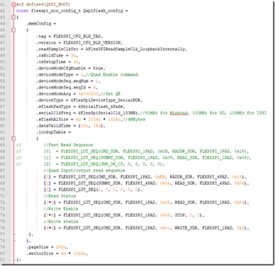
Figure 5 QSPI Flash startup mode
(1) We still take the hello world project above as an example. The previous chapters lay the foundation. This chapter is a lot easier. Under the current project, click the IAR menu bar Project->Edit Configurations to continue to create a new project configuration and HyperFlash_bootok is the blueprint, the new configuration is named "Qspi_nor_bootok" as shown below, and then click Ok to enter the configuration mode;
(2) At this time, the group file group of xip is still valid, but since the Flash type of Boot changes, it is necessary to modify the information of the first 512 bytes of Flash Configuration Parameters of the external SPI Flash (the other elements need not be modified). Open the fsl_flexspi_nor_flash.c file, and then add the following Qspiflash_config constant in front of the hyperflash_config constant (the modified source file is shown in the zip file included with this document), but actually only modified the external SPI Flash Pads type, SPI clock frequency, Flash The size (including the total size and size of the page and sector) and the most important LUT lookup table instructions, here I use the external QSPI Flash four-wire Quad I / O Read mode (ie 0xEB), the clock frequency of the SPI in this mode Can run to 133MHz, the total bandwidth can reach 532Mbps or 66.5MByte / s (in fact, many MCU on-chip Flash clock is similar to this frequency is even lower than this, but the internal Flash line width will be larger), although this speed is compared The CPU 600MHz clock speed is much slower, but in fact RT1050's L1 cache and ICache each have 32KB and are open by default in the program. Actually, for most of the code, the bandwidth of the external SPI Flash will hardly drag the CPU. Performance, complex code for specific applications left to everyone to test (measured Opus audio codec, running on external QSPI F The performance on lash is about 70%~80% running on internal SRAM);
(3) The previous step of pre-compiling QSPI_BOOT macro to enable QSPIFlash configuration information is mainly to facilitate compatibility with the previous HyperFlash startup, just add QSPI_BOOT macro in the current project configuration, as shown below, so even if you jump back HyperFlash_bootok project does not have to bother to modify the Flash Configuration Parameters element information. At the same time, the link file under the project configuration does not need to be modified because the segment address does not change. Just remember that the Keep constant should be replaced with Qspiflash_config, and then click OK to save.
(4) At this point, the configuration of the entire project is completed. Click Build to complete the compilation and linking of the entire project. Viewing the .map file also shows that the other four main element configuration information is also linked to the entire image. But the next thing that needs to be solved is the Qload Flash Flashloader problem. Support for QSPI Flash has been added to the Flashloader of IAR For ARM v8.20.2 and above, but the Flashloader only supports ISSI QSPI Flash. I have modified and optimized it to add GD and Winbond QSPI. Flash support, the new Flashloader see the zip file included with this document, copy the four files under the zip file path Firmware\IAR_8.20_Flashloader to the IAR installation directory C:\Program Files (x86)\IAR Systems\ Embedded Workbench 8.0\arm\config\flashloader\NXP and overwrite the source files. In addition, the modified Flashloader supports both the download and debug of HyperFlash and QSPI Flash (by switching the external boot mode to switch between the two programming algorithms);
(5) Everything is ready. Before clicking debug, remember to select CMSIS-DAP under options->debugger and make sure that the Reset type must select Core Reset, then click OK to save, and finally debug the code to the external QSPI Flash and debug. Or re-powered the test, hello world is still exciting, not easy, not easy.
The above two external SPI Nor Flash startup configuration methods are only taking the hello world project as an example. In fact, you can refer to the above steps to porting to other SDK instances in the SDK, and because SDK_2.3.0_EVK-MIMXRT1050\ The devices\MIMXRT1052\xip directory is a shared file (including the Flashloader is also shared), so the contents of the four files added do not need to be modified, just manually add files to the project and configure IAR related options, the operation is still Faster.
Code running in SPI Flash data running in SDRAM 3
In the previous section, we talked about the startup methods of HyperFlash and QSPI Flash, and we are eager to add some more food. I believe that in many customers developing RT105x, the code runs in the external SPI Flash, and the data stored in the external SDRAM will be a more common choice (such as some high-resolution GUI display, internal RAM) Not enough). Although the fsl_flexspi_nor_boot.c file in the four files mentioned above (two .c and two .h) has the dcd_sdram constant defined, it will soon be found that the data in this constant array is large and cannot be seen. What is the meaning (not seeing the meaning means not knowing how to modify), this is because the constant array is the compiled executable command, it is compiled according to different SDRAM results, which means different The SDRAM array is different. This is awkward. If the customer is not using the EVK onboard SDRAM, what should I do? Haha, this is not to worry, the official will soon introduce an auxiliary tool to generate DCD constant arrays of different SDRAM, but we can't wait for it before, so the "plus meal" in this chapter is to propose a workaround first. Solve this problem in advance.
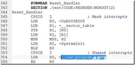
We need to know that before the system is powered on, both the code and the data are stored in the non-volatile storage medium of SPI Flash. After power-on, the program will have a Copy process to copy the data or the code that you want to execute in RAM. Inside the RAM, it doesn't matter to the internal RAM (because the internal SRAM is initialized after power-on), and for the external SDRAM, the SDRAM controller that needs to initialize the RT105x beforehand can copy the content to the SDRAM addressable space. of. Fortunately, we have a buffer time before Copy. It is precisely this buffer time gives us the opportunity to not use the DCD configuration (in fact, the DCD is also the ROM to read its contents before jumping to the application code. initialization). Take the IAR startup code as an example. Open the startup_MIMXRT1052.s file and find the CPU's starting entry Reset_Handler as shown below. The Copy process is actually implemented in the __iar_program_start function (the specific content is IAR's own library, Keil). Is implemented in __main), and before the function (that is, in the SystemInit function) we only need to initialize the SDRAM so that its Ready will not affect the copy and use of subsequent data, so I will briefly introduce the following Specific methods of operation.
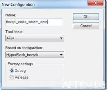
(1) Still in the current hello world project, click the IAR menu bar Project->Edit Configurations to continue to create a new project configuration and use the above HyperFlash_bootok as the blueprint to name the new configuration "flexspi_code_sdram_data" as shown below, then click Ok to enter the Configuration mode;
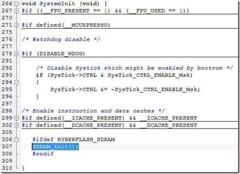
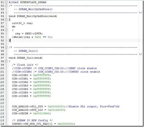
(2) Open the system_MIMXRT1052.c system configuration file, that is, the file where the SystemInit function is located, add the SDRAM initialization related function as shown below and initialize it in the last call of SystemInit before using SDRAM (specifically modified source) The file is attached to the zip file included with the document, and the initialization function is to read and write the SDRAM related registers in C language. In this way, the initialization register configuration can be modified at any time to adapt to different SDRAM even if the SDRAM is replaced. It is the most terrible, and once it is open, it is not that difficult. As for how to find the initialization of SDRAM, in fact, the command in the SDRAM preprocessing file (evkmimxrt1050_sdram_init.mac in the current directory) is implemented in C language;
(3) Since it is still for compatibility problems, the pre-compilation command is used to judge the HYBERFLASH_SDRAM macro to decide whether to initialize the SDRAM. Therefore, in the current project configuration, the HYBERFLASH_SDRAM macro declaration needs to be added to make the SDRAM initialization take effect under the current project configuration;

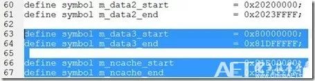
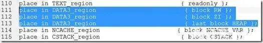
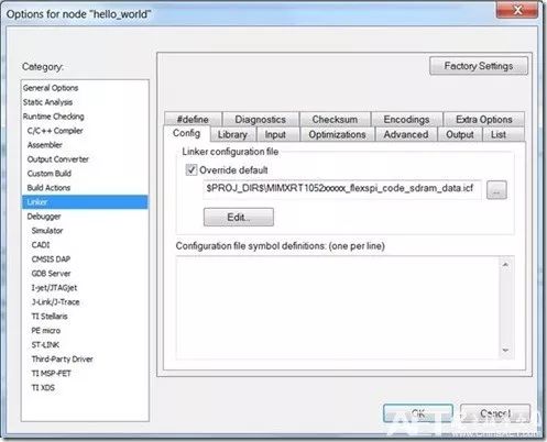
(4) Then need to modify the link file, assign the data to the SDRAM address range, copy MIMXRT1052xxxxx_hyperflash_nor_bootok.icf and rename it to MIMXRT1052xxxxx_flexspi_code_sdram_data.icf, open the file, add the data3 related information and save the link file, and in the Options -> Select the new link file in the Linker file (see the zip file included with the documentation for the source file) and click OK to save the configuration.

(5) After everything has been modified, click on the compile link, then open the .map file to see that all data variables have been allocated to the external SDRAM addressing space. Finally, click debug to download the code to the external SPI Flash. Inside (note that the SW7 boot mode remembers to change to HyperFlash startup, because this example demonstrates that code runs in HyperFlash and the data runs in SDRAM), so that the perfect implementation of the code is executed in SPI Flash and the data is run in SDRAM. Of course, hello world itself does not have much data, you can take this function according to the poring of the book to a more complex application or in the current project inside the memory alloc a large enough data area, and then read the modified write operation to test the method Reliability, I won't say much here.
GD and Winbond 3.3v QSPI Flash Boot 4
In Section 2.2, I have introduced the QIO Flash startup method for the RT1050 EVK onboard 1.8v ISSI. However, after a period of customer feedback, the QSPI Flash commonly used in the market is currently mostly GD and Winbond 3.3v products. Good quality and low price and abundant procurement channels, so I specially added the fourth chapter to introduce the GD and Winbond 3.3v QSPI Flash startup method and modify and optimize the programming algorithm of Keili to the two QSPI Flash for customers in keil. Write down and debug.
The hardware is still based on our official RT1050 EVK board as the debugging platform. Weld the ISSI QSPI Flash based on the hardware changes in Section 2.2, and replace it with GD GD25Q32CSIG 3.3v QSPI Flash (3 feet and 7 feet still pull-up resistors to VDD), then remove the 0 ohm resistor of EVK board R49 in the figure below, R301 is shorted by 0 ohm resistor, that is, the flash power is changed from the previous 1.8v to 3.3v, and other parts of the hardware are consistent with the 2.2 section, then I Introduce the configuration method in the Keil environment (the IAR used in the previous example, this time with keil let everyone familiar with the development configuration under IAR and keil):
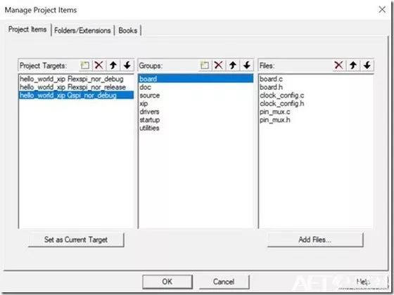
(1) First open the hello_world_xip project of the SDK development kit under Keil (path demo_apps\hello_world_xip\mdk, Keil comes with xip project), the default is only hello_world_xip Flexspi_nor_debug and hello_world_xip Flexspi_nor_release two running in the onboard HyperFlash project configuration, click the Keil menu Column Project->Manage->Project Items, we newly add a project configuration hello_world_xip Qspi_nor_debug as shown below, then select the project configuration as the current project, and finally click OK to confirm:
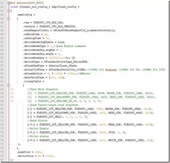
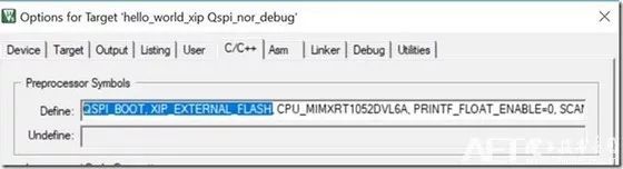
(2) In the newly created project configuration, right-click the project Options->C/C++, add the two macros QSPI_BOOT and XIP_EXTERNAL_FLASH as shown in Figure 1, then open the xip->fsl_flexspi_nor_flash.c file in the project directory, refer to section 2.2 (2 Point, manually add QSPI Flash Configuration Parameters element information as shown in Figure 2, the difference is that our official board ISSI QSPI Flash can reach up to 133MHz, while Winbond QSPI up to 80MHz, GD QSPI up to 120MHz, I I have soldered a GD GD32Q32CSIG QSPI Flash on the board, so set the serialClkFreq to kFlexSpiSerialClk_100MHz, then change the sflashA1Size to 4M Bytes;
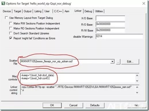
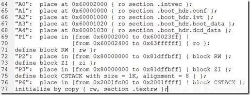
(3) Since keil comes with xip project, we can directly reuse its ready-made .scf link file without modification, as shown in Options->Linker. Moreover, Keel has also added the Keep variable to prevent the xip elements from being automatically optimized by the compiler because they are not called in the program. (Note: The following figure shows that the window is limited. In fact, the information section to be kept includes .boot_hdr.ivt , .boot_hdr.boot_data, .boot_hdr.dcd_data and .boot_hdr.conf, format reference below);
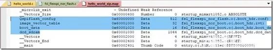
(4) At this point, we compile the entire project, and finally open the generated .map file as shown below. We can see that the element information headers that we want to start several QSPIs have been correctly allocated to the image file.
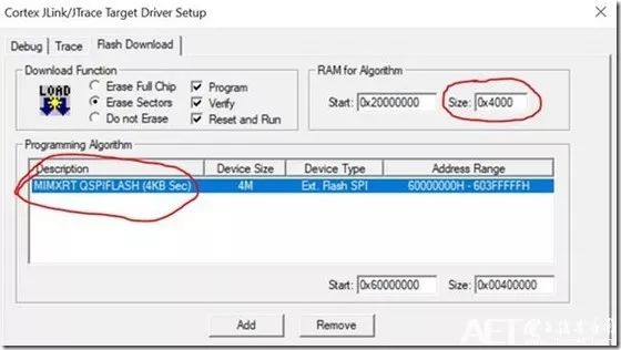
(5) The complete image file supporting QSPI startup has been solved through the above steps. Next, we need to solve the problem of QSPI Flash programming algorithm required for download, Erase and debug under keil. The path of the compressed package file attached to this document is Firmware\ The MIMXRT_QSPIFLASH.FLM file under Keil_Algorithm is the Flash algorithm that I have optimized and can support ISSI, GD and Winbond. Copy it to the keil installation path C:\Keil_v5\ARM\Flash, then right-click engineering options- >Debug-> CMSIS-DAP debugger, go to settings->Flash Download, click Add to find the MIMXRT_QSPIFLASH (4KB Sec) as shown below. It is also recommended that the RAM space reserved for the Flash algorithm is larger, otherwise the algorithm may fail. Because this flash algorithm takes up space, I have no problem changing it to 0x4000 size here;
(6) After setting, we will recompile the whole project again, then click F8 or keil menu bar Flash->Download to complete the erasing and writing of external QSPI. After the burning is finished, we can debug by clicking debug. (Recommendation: If the program has been modified, download it once before compiling into debug, and then debug), the program can be used after power off again.
ZGAR AZ Vape Pods 5.0
ZGAR electronic cigarette uses high-tech R&D, food grade disposable pod device and high-quality raw material. All package designs are Original IP. Our designer team is from Hong Kong. We have very high requirements for product quality, flavors taste and packaging design. The E-liquid is imported, materials are food grade, and assembly plant is medical-grade dust-free workshops.
From production to packaging, the whole system of tracking, efficient and orderly process, achieving daily efficient output. WEIKA pays attention to the details of each process control. The first class dust-free production workshop has passed the GMP food and drug production standard certification, ensuring quality and safety. We choose the products with a traceability system, which can not only effectively track and trace all kinds of data, but also ensure good product quality.
We offer best price, high quality Pods, Pods Touch Screen, Empty Pod System, Pod Vape, Disposable Pod device, E-cigar, Vape Pods to all over the world.
Much Better Vaping Experience!


Pods, Vape Pods, Empty Pod System Vape,Disposable Pod Vape Systems
ZGAR INTERNATIONAL(HK)CO., LIMITED , https://www.oemvape-pen.com