
TMS320C6701 (hereinafter referred to as C6701) is a floating-point arithmetic DSP, which is suitable for occasions requiring a large number of operations and high real-time requirements, such as navigation solution. In the floating-point DSP chip, the C6701 is a product that can be used in harsh environments with high reliability. Therefore, although this type of DSP chip was introduced earlier, it still has important application value in some fields.
DSP applications need to work independently of the development system. In real-time DSP applications, applications are typically stored in external non-volatile memory (such as FLASH, EEPROM, PROM, etc.). After the system is powered on, the DSP loads the program code of the external program memory into the RAM that can be accessed in high speed. After the loading is completed, it automatically jumps to the zero address and starts running. Therefore, DSP program programming and automatic loading are an important part of real-time DSP system design. The programming method used in this paper does not require format conversion to external auxiliary devices, and the DSP program no longer performs secondary loading, which simplifies the process of programming and automatic program loading.
1 loading scheme and circuit design
1.1 peripheral circuit design
The C6701 has three load modes: No Boot, ROM Boot, and Host Boot. These three load modes are set by the BOOTMODE[4:0] pin level of the C6701. The settings of these five pins together determine which memory space mapping mode to use.
In harsh environments and highly reliable applications, the no-load mode can be used, or the program can be loaded from the ROM into the DSP off-chip high-reliability RAM memory. Program memory chips such as FLASH, EEPROM, and PROM are mostly 8-bit or 16-bit, and 8-bit is more common in highly reliable application environments. In this paper, BOOTMODE[4:0] is set to 01010B, that is, the program is loaded into the external 32-bit SRAM by the external 8-bit program memory, and the LENDIAN pin is connected to the high level.
The external program memory uses FLASH chip AM29LV160, 32-bit SRAM chip selects ACT-S512K32V.FLASH and SRAM chip and C6701 hardware connection as shown in Figure 1 and Figure 2.
Figure 1 Schematic diagram of DSP and 8-bit FLASH chip interface
Figure 2 Schematic diagram of DSP and 32-bit SRAM chip interface
1.2 loading scheme design
With BOOTMODE[4:0] set to 01010B, the program is loaded into the external 32-bit SRAM by an external 8-bit program memory. The specific loading process of C6701 is as follows: DMA copies 64 KB from the CE1 address (0x01000000) to the zero-start address in the external SRAM chip according to the default timing. After the loading is completed, the execution starts from the zero address. The C6701 loading process is slightly different from the C6713. The C6713 only copies 1 KB to the zero start address. The 64 KB application can meet some application requirements. In this example, the application is less than 64 KB, and the C6701 DMA autoload can meet the requirements. When the application is larger than 64 KB, the developer needs to write a secondary bootloader that moves the DSP application from the external ROM to the specified storage space in the first 64 KB. The detailed procedure can be referenced.
2 DSP application design
A C language project usually includes. c file,. Cmd file, . Asm file, . h file and. Lib file. among them. The cmd file is both a memory location file and a linker command file that plays an important role in the linking process. When linking, the linker merges the segments of the same name in all object files and assigns addresses to the segments according to the linker command file. The interrupt vector table determines the C language program entry after the completion of loading, usually interrupt vector table. Asm file implementation. . The writing of cmd files and interrupt vector tables is the key and difficult point to determine the success of DSP program loading.
2.1 .cmd file design
. The role of the cmd file is to achieve the positioning of applications and data in the DSP mapped storage space. The allocation of storage space is closely related to the hardware design. In this paper, BOOTMODE[4:0] is 01010B, that is, the storage space is MAP0 mapping mode. The starting address of the RAM space selected by CE0 chip is 0x00000000, the starting address of the FLASH space selected by CE1 chip is 0x01000000, and the user program is less than 64KB. The cmd file is as follows:
2.2 interrupt vector table design
The interrupt vector table in this paper is as follows:
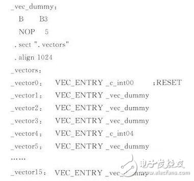
After power-on or reset is completed, the DMA copies 64 KB from the CE1 address to the zero start address at the default timing. After the loading is completed, the DSP starts from the zero address. In this paper, the interrupt vector table is stored from the program space 0 address, each interrupt vector is 8 bytes, and the total size is 0x200 bytes. After the loading is completed, the program starts from the 0 address and jumps directly to the DSP main program entry ~c_int 00.
3 programming design
After the application is written, the program needs to be programmed into the program memory. There are several methods for program burning:
1 using a general-purpose programmer for programming;
2 use CCB with its own FlashBurn tool to burn;
3 The user writes the programming program himself, and the DSP loads the application loaded on the chip into the program memory.
When programming with a general-purpose programmer, the program memory is required to be pluggable, which causes inconvenience to the design. FlashBurn supports a limited variety of memory, which may not be suitable for the use of domestic memory chips. In addition, FlashBurn does not recognize the target file, and needs to convert the target file to a binary file before burning.
It is more flexible to use the user's own method of writing programming programs. The specific method is: separately creating a programming project file, when burning, first loading the target file compiled by the application engineering into the RAM of the target DSP circuit, and then loading the target file generated by the programming project file into the target DSP circuit. In another address space of the RAM, after the main function is run, the program is executed until the programming is completed. This method of burning can avoid the coverage that may be caused by two loadings, and prevent the content of the first loading from being modified during the second loading.
3.1 programming procedures. Cmd file and interrupt vector table design
Programming program. Cmd file with user application. The cmd files are the same, but the program address allocation space must be strictly separated. In this paper, the user program address space is arranged in the 0xB400 space starting from 0, and the programming program is arranged in the 0x3400 space starting from 0xC000. Write the program. The cmd file address space is allocated as follows:
MEMORY{
VECS:o=0000C000h l=00000400h
PMEM:o=0000C400h l=00003000h
}
If you need to optimize the program space, you can compile it. The map file gets the space actually occupied by the user program and the program, and is modified. The cmd file is further optimized.
The program is not interrupted. You can only keep _c_int00. For simplicity, you can use the same interrupt vector table as the application.
3.2 programming design
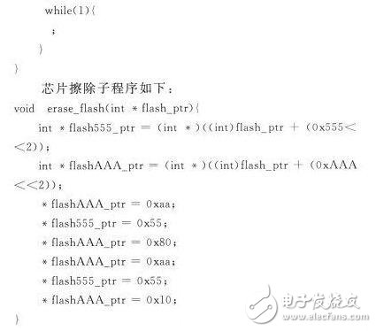
Before designing the programming program, you need to fully understand the operation process of the program memory chip. The operation code of FLASH chip AM29LV160 used in this paper has more than ten kinds of operations such as write operation, read operation, chip erase, block erase, and lock. The FLASH chip needs to be erased before the write operation. The programming procedure is as follows:
There are several points to note in programming and programming:
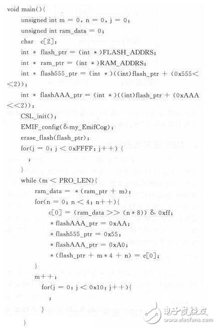
1 When programming, be sure to load the application object file into RAM first, then load the program target file into RAM, and then run the main function to perform programming.
2 FLASH_ADDRS in the program is the FLASH chip address stored in the program before auto-loading, this article is 0X01000000; RAM_ADDRS is the address stored in the program after loading, this article is the external SRAM chip address 0x00000000.
3 The EMIF needs to be initialized before the FLASH chip operation. In the program, my_EmifCog is an array of 7 32-bit binary numbers, and the seven control registers of GBLCTL, CECTL0, CECTL1, CECTL2, CECTL3, SDCTL and SDTIM are respectively configured. In this paper, CE0 is connected to the external 32-bit SRAM chip, and CE2 is connected to the 8-bit FLASH chip. CECTL0 is set to 0xFFFF3F23 and CECTL1 is 0xFFFF3F03. The other control registers need to be determined according to the application.
The 4FLASH chip can be erased in one piece or block erased, and the FLASH chip can be written after the erasing is completed. The FLASH chip has a long erase time. It is necessary to set a breakpoint after the erase subroutine, and wait for the erase to complete (you can view the 0xFF starting from 0x01000000 in CCS for reference), and then program the program.
5 PRO_LEN in the program is the length of the user program, which is the user application. The cmd file sets the total length of the interrupt vector, program, etc., which is 0xB400.
6 The external SRAM loaded into the program is 32 bits, the FLASH chip is 8 bits, and LENDIAN is high. The program that the program reads from the SRAM is 32 bits, and the 32-bit data needs to be programmed into the 8-bit FLASH chip in order from low to high.
Conclusion
The practical engineering application verified the feasibility of the above-mentioned programming and automatic loading methods. The loading process described in this paper saves the DSP system startup time compared to the secondary loading, but the FLASH chip read and write waiting time is the default setting during the loading process, the user cannot change, the program loading time is still 120 ms, in some watchdogs. Special considerations are needed in applications with shorter timelines. The program burning method of this paper can also be applied to other DSP systems.
Rotary encoders are used as sensors for angle,position,speed and acceleration. We can offer incremental encoders and absolute encoders.

Absolute Encoder,Custom Encoder On Motor,Custom Optical Encoders,High Resolution Encoder
Yuheng Optics Co., Ltd.(Changchun) , https://www.yuhengcoder.com