
When implementing the transition from 10G to 25G systems for next-generation servers and switches, hardware design engineers must meet these goals: minimize data latency, maintain or reduce power consumption, and minimize cost. In order to provide data center users with world-class cost-effective products, fundamentally, more must be done at a small cost.
Here are 5 tips to make a good balance when designing a 25G system:
1. Determining which link in the system will require signal conditioning; this will depend on the trace length and printed circuit board (PCB) material. Low loss materials require less signal conditioning, but they are also more expensive than standard materials. Channels that deplete more than the inherent compensation function of an application specific integrated circuit (ASIC) will require some form of signal conditioning. For example, if your ASIC is capable of 30dB compensation, you may want to add signal conditioning to channels with losses of 27dB or more, and a 3dB difference can be used as a safety margin. Figure 1 is a diagram showing a comparison of channel loss budget analysis between PCB materials A and B.
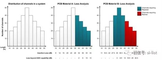
Figure 1: An example distribution of channels within a system,
Assume ASIC loss compensation capability: 30dB at 12.9GHz, PCB material A loss: 0.8dB per inch at 12.9GHz, PCB material B loss: 1.1dB per inch at 12.9GHz.
2. Design flexibility in small packages for channels that require signal conditioning. The small package provides high channel density and allows you to use retimers or pin-compatible repeaters.
3. Design a power solution that meets the needs of a retimer or repeater. For example, the TPS53513 synchronous buck converter can provide 8A current, which is enough for a set of 6 retimers or repeaters.
4. Determine the SMBus addressing mechanism, which requires separate addressing of each retimer/repeater device on the board. You can select one of the 16 unique SMBus addresses for each device's pin configuration. If there are more than 16 devices on a single board, consider using an I2C expander such as the TCA/PCA Series I2C/SMBus switch to divide the SMBus into multiple buses.
5. Place a single low-cost 25MHz (±100ppm) 2.5V single-ended clock on the board to support up to 20 retimer devices. Since it is not used to recover data, this clock does not require any jitter. This retimer buffers the receive clock for timing, buffers it, and copies it on an output pin for easy cascading to the next retimer. No need to use multiple crystals or fanout buffers. If you finally decide to use a repeater instead of a retimer, then you can choose not to assemble this component to reduce costs.
To make these tips simpler to implement, TI has introduced the industry's first pin-compatible repeater (DS280BR810) and retimer (DS250DF810) solution portfolio for 25G backplane and front port applications. And how do these help achieve a balance between power, performance, and cost? All of this is related to design simplicity and flexibility.
TI's pin-compatible repeater and retimer solutions allow you to choose a solution that meets your performance goals while minimizing latency and bill of materials (BOM) costs. Hardware engineers know that the cost, size, and complexity of the surrounding components are just as important as the repeater or retimer itself. Consider the board design example in Figure 2.
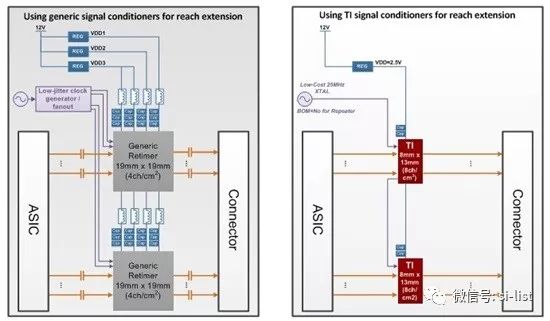
Figure 2: illustrates the simplicity and cost savings of a TI solution (right side) versus a common solution (left side)
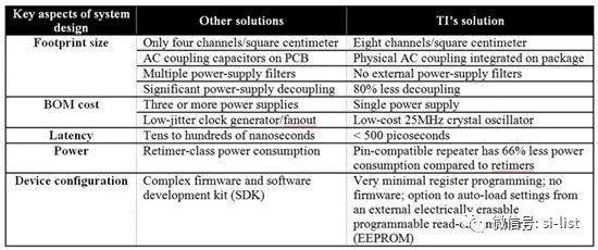
Table 1: Comparison of TI's 25G Signal Conditioning Solution and Other Solutions
The pin-compatible nature of TI's 25G DS280BR810 repeater and DS250DF810 retimer solution allows you to generate a schematic to evaluate these two options for cost, power, and performance optimization for the final product. Signal integrity engineers can start testing with a repeater solution that provides lower cost and power. If jitter and crosstalk in the system require higher performance, they can be upgraded to a pin-compatible retimer solution.
Small optimizations are really important. Imagine a typical data center with 20,000 servers. Using a repeater instead of a retimer can save a server network interface card (NIC) by about 1 watt of power, adding up to an annual savings of more than $21,000 ($0.12 per kWh), which is not yet Includes the savings in cooling savings. If you reduce the BOM component cost by $5, you can save an extra $100,000. Finally, the difference between the 50ns delay and the 500ps delay is that while the entire data center service request is met, it is “wasted†for 8 hours per day (assuming there are 2000 requests per second, the total usage time per server per day is 4 hours).
By using these tips, you should be able to design a board that balances cost, power, and performance.
Wall Power Switch And Socket,Remote Control Electrical Outlet,Battery Powered Light Switch,Electrical Outlet With Switch
ZHEJIANG HUAYAN ELECTRIC CO.,LTD , https://www.huayanelectric.com